Development in general requires time and money. Development of opensource projects is not an exception. To keep this online resource alive we heavily rely on your donations. If you feel like supporting us please make a donation.
Zynq and Ultrascale MPSoCs from Xilinx are very rich and flexible in terms of peripherals, both SoCs are equipped with HS/FS USB host hardware blocks. While those are fully supported by the Petalinux, for reasons unknown there is still no software support for USB host functionality when it comes to baremetal or FreeRTOS. The standard board support packages from Xilinx support only device mode but no host.
At the same time, Petalinux simply can’t be the ultimate answer to any development challenge as there is still need for lightweight, compact applications capable of booting in just a matter of couple of seconds yet requiring USB host functionality. At the time of working on this example there was (and still is) literally no any existing solution in the world of this kind so there is hope that from now developers will have at least one option.
USB Host stack integration
To avoid development of a whole USB stack from scratch already existing one was chosen. It is called TinyUSB, it has small footprint and is fully written in C with cross platform idea in mind, it also has a non-restrictive MIT licence. As a downside, it doesn’t have support for Xilinx SoCs. To overcome this, we have designed ‘Zynq 7000 glue logic’ which resides between the hardware and the USB stack as it is shown on the picture below.
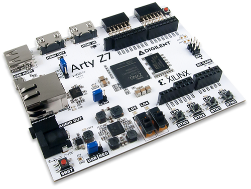
We are presenting a fully functional proof of concept application with integrated USB Host 2.0 stack featuring the TinyUSB third party library and HID driver for Zynq 7000 powered systems. Our project targets ARTY Z7 boards with Zynq7000 MPSoCs and Vivado 2017.3 development environment. However, this concept could be transferred to virtually any version of Vivado, besides, the approach will work equally well for Ultrascale family as well.
We are offering this solution for a flat price of 24.99 USD which can be paid by Paypal.
What do you get after payment?
Full source code of the working proof of concept USB Host example with a HID driver including integration layer with the TinyUSB third part library;
Set of TCL scripts for building PL and PS projects resulting in *.bin files with embedded first stage boot loader;
Documentation in pdf format;
Technical support over email/telegram channel;
NOTE: please allow some time for processing as we are working on logistic automation. In case of any concern please contact us.
Video tutorial
A walk-through of the project with fully integrated USB Host stack and HID keyboard example in the form of a video tutorial is provided below:
Have you ever experienced limitations of the Zynq/Ultrascale MPSoCs from Xilinx when it comes to GEMs and MDIO interfaces? The thing is that only specific GPIO pins can be used for MDIO communication. As seen on the picture below, apart from EMIO (PL pins) only MIO 52 and 53 can be used to drive a PHY chip on ENET 0. Besides, those MIO 52 and 53 can’t be used for ENET 1.
So what happens if you have fully exhausted EMIO pins in your design? Or due to some circumstance MIO 52 and 53 can’t be used? Or by mistake some other MIO pins have been routed to the PHY chip, is there any way to make it work? Actually, there is. In fact, there is a solution to drive MDIO interface by means of any GPIO pin, be it MIO or EMIO. The idea is to drive any two GPIO pins the same way the MDIO hardware block does. And then simply remap the EMAC driver to use our own functions for reading and writing PHY registers while disabling the MDIO hardware block. Now there is an alternative way of driving a PHY as it is shown on the picture below.
Why it is so important to communicate to PHY you may ask. It doesn’t have to be actively driven if it is impossible or difficult to do so, instead, a PHY chip could be configured by boot strap resistors. That is true but there are some caveats:
Boot strap resistors configure PHY chips to work in one fixed mode, be it 10Mbps, 100Mbps, 1Gbps or auto negotiation mode. Once a mode is chosen it can’t be changed without hardware modifications;
Boot strap resistors don’t solve the problem of communication with a PHY which means that in this case hardware won’t generate LINK UP / LINK DOWN events and our software stack will be totally unaware of a presence or absence of a physical link;
Suggested solution
We are presenting a fully functional proof of concept application which demonstrates a feasibility of driving MDIO/MDC lines via any GPIO pins for Zynq/Ultrascale powered systems. Our project targets ARTY Z7 boards with Zynq7000 MPSoCs and Vivado 2017.3 development environment. However, this concept could be transferred to virtually any version of Vivado, besides, the approach will work equally well for Ultrascale family as well.
We are offering this solution for a flat price of 24.99 USD which can be paid by Paypal.
What do you get after payment?
Full source code of the working proof of concept example with echo TCP service including MDIO over GPIO driver;
Set of TCL scripts for building PL and PS projects resulting in *.bin files with embedded first stage boot loader;
Documentation in pdf format;
Technical support over email/telegram channel;
NOTE: please allow some time for processing as we are working on logistic automation. In case of any concern please contact us.
Video tutorial
A walk-through of the project demonstrating how to drive MDIO lines by software driver in the form of a video tutorial is provided below:
In this tutorial we are going to use the same hardware descriptor from the previous post and build an RGB LED PWM Demo driven by Petalinux. To do this we will need a Linux machine with Petalinux SDK installed on it. In this experiment we will be using SDK 2017.3 but any newer revisions up to 2020.1 should work equally well.
The process of Petalinux project creation and building is described in many places including UG1144 Reference Guide so let’s focus of specific things which will be implemented in our project.
First of all, LED control will be done through a web interface. Each colour intensity for each of the two RGB LEDs will be controlled independently by a slider. Going through the intricacies of web design is out of scope of this tutorial, instead, only most important things will be highlighted.
The slider is going to be extremely simplistic and fully implemented in the form of Stylesheets. It is defined in a separate file slider.css, the full content of which is given below:
The slider is instantiated six times (three colours per each LED) in index.html as it is shown below. There are also JavaScript functions attached to each slider and triggering upon change in slider’s position. Every time when position of any slider changes a set_led function is invoked. To make the page more interactive, there is logic to change font colour of led0_caption and led1_caption by mixing the values of the three base colours selected by appropriate sliders.
The implementation of set_led JavaScript function is in config.js, the fragment of the file is given below. The function makes asynchronous call which in its turn executes rgb-led-pwm shell script located in cgi-bin folder. The script also gets two parameters, a register name and a value.
The rgb-led-pwm shell script parses parameters passed by the browser translates the register name into address. With the help of the devmem tool it writes the value at a given address which is in essence writing value into a register. The script then responds with status in JSON format to keep the web browser happy.
There is one more custom made shell script bootscript given below. It is going to be ran upon Linux boot and start httpd daemon to serve web pages at port 8080. There are also initial values to be written to all registers of our PWM AXI block which has been implemented in FPGA fabric earlier. The fundamental difference between Linux and bare-metal or real time OS is that Linux user applications are running in virtual address spaces so any attempt to access physical registers will inevitably cause well-known segmentation fault as the kernel prevents applications from accessing resources outside of the allowed address space. There are several ways to deal with this, in this project we will be using devmem tool which allows to access registers correctly.
The final version of a customised Yocto script bootscript.bb is given below. It packages our webpage and its resources including JavaScripts, StyleSheets, images and GGI scripts into root file system.
The final look of the web interface is given below. There are two LEDs and six sliders controlling intensity of base colour for each of the LEDs. As it is seen, the LED 0 is of red colour (only red slider has non-zero value) and the LED 1 is of light blue (which is a mix of green and blue encoded by two sliders):
RGB LED PWM Demo on Petalinux webpage Screenshot
Video tutorial:
The complete process of creating a Petalinux project and building a bootable image for QSPI flash is given below:
Having hardware and software configurable platform gives the ultimate flexibility. Having FPGA fabric and two ARM cores integrated into a single System-On-Chip (SoC) gives benefits of the two (hardware and software) worlds, compact size, advanced optimisation of such integration, reduces the time for development effort, simplifies subsequent testing, verification and validation. Today we are reviewing a great development platform with Zynq 7020 SoC from Xilinx. Let’s implement an equivalent of ‘Hello World’ application, in our case we are going to create 6 independent PWM channels in hardware, connect them to the two RGB LEDs and write a simple demo cycling through the colours.
The board that we are going to use is Arty Z7-20, its picture is given below:
We will also need a Vivado Webpack SDK, we will be using relatively old but stable revision 2017.3 but our readers have a full freedom of using something more recent. At the end of the day, the tool doesn’t matter as much as the actual engineer who uses the tool.
Let’s iterate through the steps of our activities. We are going to create a blank Vivado project, create a board design, design a new AXI IP core which will control our PWM channels through the set of registers, go back to the main project, create a Zynq processing system, enable board’s system clock and RGB LED peripheral and connect it to the processing system through our newly designed PWM IP Core. Then add constraints, generate HDL wrapper, synthesize and run the implementation, generate bitstream and hardware description, export it to SDK, create an empty FreeRTOS application, write our C code for controlling LEDs and then run the demo.
There is not so much of the code writing during this exercise, it is customising VHDL template for the AXI IP Core and C-code. Let’s start by looking at the VHDL code.
First code example is given below, it is autogenerated led_pwm_v1_0.vhd that acts as a wrapper around the AXI Bus Interface. The highlighted lines are our customised additions to the autogenerated code:
library ieee;
use ieee.std_logic_1164.all;
use ieee.numeric_std.all;
entity led_pwm_v1_0 is
	generic (
		-- Users to add parameters here
		-- User parameters ends
		-- Do not modify the parameters beyond this line
		-- Parameters of Axi Slave Bus Interface S00_AXI
		C_S00_AXI_DATA_WIDTH	: integer	:= 32;
		C_S00_AXI_ADDR_WIDTH	: integer	:= 5
	);
	port (
		-- Users to add ports here
		gpio_io_o : out std_logic_vector(5 downto 0);
		-- User ports ends
		-- Do not modify the ports beyond this line
		-- Ports of Axi Slave Bus Interface S00_AXI
		s00_axi_aclk	: in std_logic;
		s00_axi_aresetn	: in std_logic;
		s00_axi_awaddr	: in std_logic_vector(C_S00_AXI_ADDR_WIDTH-1 downto 0);
		s00_axi_awprot	: in std_logic_vector(2 downto 0);
		s00_axi_awvalid	: in std_logic;
		s00_axi_awready	: out std_logic;
		s00_axi_wdata	: in std_logic_vector(C_S00_AXI_DATA_WIDTH-1 downto 0);
		s00_axi_wstrb	: in std_logic_vector((C_S00_AXI_DATA_WIDTH/8)-1 downto 0);
		s00_axi_wvalid	: in std_logic;
		s00_axi_wready	: out std_logic;
		s00_axi_bresp	: out std_logic_vector(1 downto 0);
		s00_axi_bvalid	: out std_logic;
		s00_axi_bready	: in std_logic;
		s00_axi_araddr	: in std_logic_vector(C_S00_AXI_ADDR_WIDTH-1 downto 0);
		s00_axi_arprot	: in std_logic_vector(2 downto 0);
		s00_axi_arvalid	: in std_logic;
		s00_axi_arready	: out std_logic;
		s00_axi_rdata	: out std_logic_vector(C_S00_AXI_DATA_WIDTH-1 downto 0);
		s00_axi_rresp	: out std_logic_vector(1 downto 0);
		s00_axi_rvalid	: out std_logic;
		s00_axi_rready	: in std_logic
	);
end led_pwm_v1_0;
architecture arch_imp of led_pwm_v1_0 is
	-- component declaration
	component led_pwm_v1_0_S00_AXI is
		generic (
		C_S_AXI_DATA_WIDTH	: integer	:= 32;
		C_S_AXI_ADDR_WIDTH	: integer	:= 5
		);
		port (
		rgb_led_tri_o : out std_logic_vector(5 downto 0);
		S_AXI_ACLK	: in std_logic;
		S_AXI_ARESETN	: in std_logic;
		S_AXI_AWADDR	: in std_logic_vector(C_S_AXI_ADDR_WIDTH-1 downto 0);
		S_AXI_AWPROT	: in std_logic_vector(2 downto 0);
		S_AXI_AWVALID	: in std_logic;
		S_AXI_AWREADY	: out std_logic;
		S_AXI_WDATA	: in std_logic_vector(C_S_AXI_DATA_WIDTH-1 downto 0);
		S_AXI_WSTRB	: in std_logic_vector((C_S_AXI_DATA_WIDTH/8)-1 downto 0);
		S_AXI_WVALID	: in std_logic;
		S_AXI_WREADY	: out std_logic;
		S_AXI_BRESP	: out std_logic_vector(1 downto 0);
		S_AXI_BVALID	: out std_logic;
		S_AXI_BREADY	: in std_logic;
		S_AXI_ARADDR	: in std_logic_vector(C_S_AXI_ADDR_WIDTH-1 downto 0);
		S_AXI_ARPROT	: in std_logic_vector(2 downto 0);
		S_AXI_ARVALID	: in std_logic;
		S_AXI_ARREADY	: out std_logic;
		S_AXI_RDATA	: out std_logic_vector(C_S_AXI_DATA_WIDTH-1 downto 0);
		S_AXI_RRESP	: out std_logic_vector(1 downto 0);
		S_AXI_RVALID	: out std_logic;
		S_AXI_RREADY	: in std_logic
		);
	end component led_pwm_v1_0_S00_AXI;
begin
-- Instantiation of Axi Bus Interface S00_AXI
led_pwm_v1_0_S00_AXI_inst : led_pwm_v1_0_S00_AXI
	generic map (
		C_S_AXI_DATA_WIDTH	=> C_S00_AXI_DATA_WIDTH,
		C_S_AXI_ADDR_WIDTH	=> C_S00_AXI_ADDR_WIDTH
	)
	port map (
		rgb_led_tri_o => gpio_io_o,
		S_AXI_ACLK	=> s00_axi_aclk,
		S_AXI_ARESETN	=> s00_axi_aresetn,
		S_AXI_AWADDR	=> s00_axi_awaddr,
		S_AXI_AWPROT	=> s00_axi_awprot,
		S_AXI_AWVALID	=> s00_axi_awvalid,
		S_AXI_AWREADY	=> s00_axi_awready,
		S_AXI_WDATA	=> s00_axi_wdata,
		S_AXI_WSTRB	=> s00_axi_wstrb,
		S_AXI_WVALID	=> s00_axi_wvalid,
		S_AXI_WREADY	=> s00_axi_wready,
		S_AXI_BRESP	=> s00_axi_bresp,
		S_AXI_BVALID	=> s00_axi_bvalid,
		S_AXI_BREADY	=> s00_axi_bready,
		S_AXI_ARADDR	=> s00_axi_araddr,
		S_AXI_ARPROT	=> s00_axi_arprot,
		S_AXI_ARVALID	=> s00_axi_arvalid,
		S_AXI_ARREADY	=> s00_axi_arready,
		S_AXI_RDATA	=> s00_axi_rdata,
		S_AXI_RRESP	=> s00_axi_rresp,
		S_AXI_RVALID	=> s00_axi_rvalid,
		S_AXI_RREADY	=> s00_axi_rready
	);
	-- Add user logic here
	-- User logic ends
end arch_imp;
Second code example is autogenerated led_pwm_ip_v3_0_S00_AXI.vhd which is the actual the AXI Bus Interface. Once again, the highlighted lines are manual additions to the autogenerated code. The code is modified to give more meaningful names to the four slave registers accessible through the ARM CPU, these are the code and the registers:
library ieee;
use ieee.std_logic_1164.all;
use ieee.numeric_std.all;
entity led_pwm_v1_0_S00_AXI is
	generic (
		-- Users to add parameters here
		-- User parameters ends
		-- Do not modify the parameters beyond this line
		-- Width of S_AXI data bus
		C_S_AXI_DATA_WIDTH	: integer	:= 32;
		-- Width of S_AXI address bus
		C_S_AXI_ADDR_WIDTH	: integer	:= 5
	);
	port (
		-- Users to add ports here
		rgb_led_tri_o : out std_logic_vector(5 downto 0);
		-- User ports ends
		-- Do not modify the ports beyond this line
		-- Global Clock Signal
		S_AXI_ACLK	: in std_logic;
		-- Global Reset Signal. This Signal is Active LOW
		S_AXI_ARESETN	: in std_logic;
		-- Write address (issued by master, acceped by Slave)
		S_AXI_AWADDR	: in std_logic_vector(C_S_AXI_ADDR_WIDTH-1 downto 0);
		-- Write channel Protection type. This signal indicates the
    		-- privilege and security level of the transaction, and whether
    		-- the transaction is a data access or an instruction access.
		S_AXI_AWPROT	: in std_logic_vector(2 downto 0);
		-- Write address valid. This signal indicates that the master signaling
    		-- valid write address and control information.
		S_AXI_AWVALID	: in std_logic;
		-- Write address ready. This signal indicates that the slave is ready
    		-- to accept an address and associated control signals.
		S_AXI_AWREADY	: out std_logic;
		-- Write data (issued by master, acceped by Slave)
		S_AXI_WDATA	: in std_logic_vector(C_S_AXI_DATA_WIDTH-1 downto 0);
		-- Write strobes. This signal indicates which byte lanes hold
    		-- valid data. There is one write strobe bit for each eight
    		-- bits of the write data bus.
		S_AXI_WSTRB	: in std_logic_vector((C_S_AXI_DATA_WIDTH/8)-1 downto 0);
		-- Write valid. This signal indicates that valid write
    		-- data and strobes are available.
		S_AXI_WVALID	: in std_logic;
		-- Write ready. This signal indicates that the slave
    		-- can accept the write data.
		S_AXI_WREADY	: out std_logic;
		-- Write response. This signal indicates the status
    		-- of the write transaction.
		S_AXI_BRESP	: out std_logic_vector(1 downto 0);
		-- Write response valid. This signal indicates that the channel
    		-- is signaling a valid write response.
		S_AXI_BVALID	: out std_logic;
		-- Response ready. This signal indicates that the master
    		-- can accept a write response.
		S_AXI_BREADY	: in std_logic;
		-- Read address (issued by master, acceped by Slave)
		S_AXI_ARADDR	: in std_logic_vector(C_S_AXI_ADDR_WIDTH-1 downto 0);
		-- Protection type. This signal indicates the privilege
    		-- and security level of the transaction, and whether the
    		-- transaction is a data access or an instruction access.
		S_AXI_ARPROT	: in std_logic_vector(2 downto 0);
		-- Read address valid. This signal indicates that the channel
    		-- is signaling valid read address and control information.
		S_AXI_ARVALID	: in std_logic;
		-- Read address ready. This signal indicates that the slave is
    		-- ready to accept an address and associated control signals.
		S_AXI_ARREADY	: out std_logic;
		-- Read data (issued by slave)
		S_AXI_RDATA	: out std_logic_vector(C_S_AXI_DATA_WIDTH-1 downto 0);
		-- Read response. This signal indicates the status of the
    		-- read transfer.
		S_AXI_RRESP	: out std_logic_vector(1 downto 0);
		-- Read valid. This signal indicates that the channel is
    		-- signaling the required read data.
		S_AXI_RVALID	: out std_logic;
		-- Read ready. This signal indicates that the master can
    		-- accept the read data and response information.
		S_AXI_RREADY	: in std_logic
	);
end led_pwm_v1_0_S00_AXI;
architecture arch_imp of led_pwm_v1_0_S00_AXI is
        component pwm is
            generic (
               G_DATA_WIDTH : integer := 32);
            port (
                f_aclk : in std_logic;
                i_aresetn : in std_logic;
                i_pwm_module : in std_logic_vector(C_S_AXI_DATA_WIDTH - 1 downto 0);
                i_pwm_width : in std_logic_vector(C_S_AXI_DATA_WIDTH - 1 downto 0);
                o_pwm : out std_logic);
        end component;
	-- AXI4LITE signals
	signal axi_awaddr	: std_logic_vector(C_S_AXI_ADDR_WIDTH-1 downto 0);
	signal axi_awready	: std_logic;
	signal axi_wready	: std_logic;
	signal axi_bresp	: std_logic_vector(1 downto 0);
	signal axi_bvalid	: std_logic;
	signal axi_araddr	: std_logic_vector(C_S_AXI_ADDR_WIDTH-1 downto 0);
	signal axi_arready	: std_logic;
	signal axi_rdata	: std_logic_vector(C_S_AXI_DATA_WIDTH-1 downto 0);
	signal axi_rresp	: std_logic_vector(1 downto 0);
	signal axi_rvalid	: std_logic;
	-- Example-specific design signals
	-- local parameter for addressing 32 bit / 64 bit C_S_AXI_DATA_WIDTH
	-- ADDR_LSB is used for addressing 32/64 bit registers/memories
	-- ADDR_LSB = 2 for 32 bits (n downto 2)
	-- ADDR_LSB = 3 for 64 bits (n downto 3)
	constant ADDR_LSB  : integer := (C_S_AXI_DATA_WIDTH/32)+ 1;
	constant OPT_MEM_ADDR_BITS : integer := 2;
	------------------------------------------------
	---- Signals for user logic register space example
	--------------------------------------------------
	---- Number of Slave Registers 7
        signal i_pwm_module :std_logic_vector(C_S_AXI_DATA_WIDTH-1 downto 0);
        signal i_pwm_width0 :std_logic_vector(C_S_AXI_DATA_WIDTH-1 downto 0);
        signal i_pwm_width1 :std_logic_vector(C_S_AXI_DATA_WIDTH-1 downto 0);
        signal i_pwm_width2 :std_logic_vector(C_S_AXI_DATA_WIDTH-1 downto 0);
        signal i_pwm_width3 :std_logic_vector(C_S_AXI_DATA_WIDTH-1 downto 0);
        signal i_pwm_width4 :std_logic_vector(C_S_AXI_DATA_WIDTH-1 downto 0);
        signal i_pwm_width5 :std_logic_vector(C_S_AXI_DATA_WIDTH-1 downto 0);
	signal slv_reg_rden	: std_logic;
	signal slv_reg_wren	: std_logic;
	signal reg_data_out	:std_logic_vector(C_S_AXI_DATA_WIDTH-1 downto 0);
	signal byte_index	: integer;
	signal aw_en	: std_logic;
begin
        pwm1: pwm
            generic map (
                G_DATA_WIDTH => C_S_AXI_DATA_WIDTH
            )
            port map (
                f_aclk => S_AXI_ACLK,
                i_aresetn => S_AXI_ARESETN,
                i_pwm_module => i_pwm_module,
                i_pwm_width => i_pwm_width0,
                o_pwm => rgb_led_tri_o(0)
            );
        pwm2: pwm
            generic map (
                G_DATA_WIDTH => C_S_AXI_DATA_WIDTH
            )
            port map (
                f_aclk => S_AXI_ACLK,
                i_aresetn => S_AXI_ARESETN,
                i_pwm_module => i_pwm_module,
                i_pwm_width => i_pwm_width1,
                o_pwm => rgb_led_tri_o(1)
            );
        pwm3: pwm
            generic map (
                G_DATA_WIDTH => C_S_AXI_DATA_WIDTH
            )
            port map (
                f_aclk => S_AXI_ACLK,
                i_aresetn => S_AXI_ARESETN,
                i_pwm_module => i_pwm_module,
                i_pwm_width => i_pwm_width2,
                o_pwm => rgb_led_tri_o(2)
            );
        pwm4: pwm
            generic map (
                G_DATA_WIDTH => C_S_AXI_DATA_WIDTH
            )
            port map (
                f_aclk => S_AXI_ACLK,
                i_aresetn => S_AXI_ARESETN,
                i_pwm_module => i_pwm_module,
                i_pwm_width => i_pwm_width3,
                o_pwm => rgb_led_tri_o(3)
            );
        pwm5: pwm
            generic map (
                G_DATA_WIDTH => C_S_AXI_DATA_WIDTH
            )
            port map (
                f_aclk => S_AXI_ACLK,
                i_aresetn => S_AXI_ARESETN,
                i_pwm_module => i_pwm_module,
                i_pwm_width => i_pwm_width4,
                o_pwm => rgb_led_tri_o(4)
            );
        pwm6: pwm
            generic map (
                G_DATA_WIDTH => C_S_AXI_DATA_WIDTH
            )
            port map (
                f_aclk => S_AXI_ACLK,
                i_aresetn => S_AXI_ARESETN,
                i_pwm_module => i_pwm_module,
                i_pwm_width => i_pwm_width5,
                o_pwm => rgb_led_tri_o(5)
            );
	-- I/O Connections assignments
	S_AXI_AWREADY	<= axi_awready;
	S_AXI_WREADY	<= axi_wready;
	S_AXI_BRESP	<= axi_bresp;
	S_AXI_BVALID	<= axi_bvalid;
	S_AXI_ARREADY	<= axi_arready;
	S_AXI_RDATA	<= axi_rdata;
	S_AXI_RRESP	<= axi_rresp;
	S_AXI_RVALID	<= axi_rvalid;
	-- Implement axi_awready generation
	-- axi_awready is asserted for one S_AXI_ACLK clock cycle when both
	-- S_AXI_AWVALID and S_AXI_WVALID are asserted. axi_awready is
	-- de-asserted when reset is low.
	process (S_AXI_ACLK)
	begin
	  if rising_edge(S_AXI_ACLK) then
	    if S_AXI_ARESETN = '0' then
	      axi_awready <= '0';
	      aw_en <= '1';
	    else
	      if (axi_awready = '0' and S_AXI_AWVALID = '1' and S_AXI_WVALID = '1' and aw_en = '1') then
	        -- slave is ready to accept write address when
	        -- there is a valid write address and write data
	        -- on the write address and data bus. This design
	        -- expects no outstanding transactions.
	        axi_awready <= '1';
	        elsif (S_AXI_BREADY = '1' and axi_bvalid = '1') then
	            aw_en <= '1';
	        	axi_awready <= '0';
	      else
	        axi_awready <= '0';
	      end if;
	    end if;
	  end if;
	end process;
	-- Implement axi_awaddr latching
	-- This process is used to latch the address when both
	-- S_AXI_AWVALID and S_AXI_WVALID are valid.
	process (S_AXI_ACLK)
	begin
	  if rising_edge(S_AXI_ACLK) then
	    if S_AXI_ARESETN = '0' then
	      axi_awaddr <= (others => '0');
	    else
	      if (axi_awready = '0' and S_AXI_AWVALID = '1' and S_AXI_WVALID = '1' and aw_en = '1') then
	        -- Write Address latching
	        axi_awaddr <= S_AXI_AWADDR;
	      end if;
	    end if;
	  end if;
	end process;
	-- Implement axi_wready generation
	-- axi_wready is asserted for one S_AXI_ACLK clock cycle when both
	-- S_AXI_AWVALID and S_AXI_WVALID are asserted. axi_wready is
	-- de-asserted when reset is low.
	process (S_AXI_ACLK)
	begin
	  if rising_edge(S_AXI_ACLK) then
	    if S_AXI_ARESETN = '0' then
	      axi_wready <= '0';
	    else
	      if (axi_wready = '0' and S_AXI_WVALID = '1' and S_AXI_AWVALID = '1' and aw_en = '1') then
	          -- slave is ready to accept write data when
	          -- there is a valid write address and write data
	          -- on the write address and data bus. This design
	          -- expects no outstanding transactions.
	          axi_wready <= '1';
	      else
	        axi_wready <= '0';
	      end if;
	    end if;
	  end if;
	end process;
	-- Implement memory mapped register select and write logic generation
	-- The write data is accepted and written to memory mapped registers when
	-- axi_awready, S_AXI_WVALID, axi_wready and S_AXI_WVALID are asserted. Write strobes are used to
	-- select byte enables of slave registers while writing.
	-- These registers are cleared when reset (active low) is applied.
	-- Slave register write enable is asserted when valid address and data are available
	-- and the slave is ready to accept the write address and write data.
	slv_reg_wren <= axi_wready and S_AXI_WVALID and axi_awready and S_AXI_AWVALID ;
	process (S_AXI_ACLK)
	variable loc_addr :std_logic_vector(OPT_MEM_ADDR_BITS downto 0);
	begin
	  if rising_edge(S_AXI_ACLK) then
	    if S_AXI_ARESETN = '0' then
                i_pwm_module <= (others => '0');
                i_pwm_width0 <= (others => '0');
                i_pwm_width1 <= (others => '0');
                i_pwm_width2 <= (others => '0');
                i_pwm_width3 <= (others => '0');
                i_pwm_width4 <= (others => '0');
                i_pwm_width5 <= (others => '0');
	    else
	      loc_addr := axi_awaddr(ADDR_LSB + OPT_MEM_ADDR_BITS downto ADDR_LSB);
	      if (slv_reg_wren = '1') then
	        case loc_addr is
	          when b"000" =>
	            for byte_index in 0 to (C_S_AXI_DATA_WIDTH/8-1) loop
	              if ( S_AXI_WSTRB(byte_index) = '1' ) then
	                -- Respective byte enables are asserted as per write strobes
	                -- slave registor 0
	                i_pwm_module(byte_index*8+7 downto byte_index*8) <= S_AXI_WDATA(byte_index*8+7 downto byte_index*8);
	              end if;
	            end loop;
	          when b"001" =>
	            for byte_index in 0 to (C_S_AXI_DATA_WIDTH/8-1) loop
	              if ( S_AXI_WSTRB(byte_index) = '1' ) then
	                -- Respective byte enables are asserted as per write strobes
	                -- slave registor 1
	                i_pwm_width0(byte_index*8+7 downto byte_index*8) <= S_AXI_WDATA(byte_index*8+7 downto byte_index*8);
	              end if;
	            end loop;
	          when b"010" =>
	            for byte_index in 0 to (C_S_AXI_DATA_WIDTH/8-1) loop
	              if ( S_AXI_WSTRB(byte_index) = '1' ) then
	                -- Respective byte enables are asserted as per write strobes
	                -- slave registor 2
	                i_pwm_width1(byte_index*8+7 downto byte_index*8) <= S_AXI_WDATA(byte_index*8+7 downto byte_index*8);
	              end if;
	            end loop;
	          when b"011" =>
	            for byte_index in 0 to (C_S_AXI_DATA_WIDTH/8-1) loop
	              if ( S_AXI_WSTRB(byte_index) = '1' ) then
	                -- Respective byte enables are asserted as per write strobes
	                -- slave registor 3
	                i_pwm_width2(byte_index*8+7 downto byte_index*8) <= S_AXI_WDATA(byte_index*8+7 downto byte_index*8);
	              end if;
	            end loop;
	          when b"100" =>
	            for byte_index in 0 to (C_S_AXI_DATA_WIDTH/8-1) loop
	              if ( S_AXI_WSTRB(byte_index) = '1' ) then
	                -- Respective byte enables are asserted as per write strobes
	                -- slave registor 4
	                i_pwm_width3(byte_index*8+7 downto byte_index*8) <= S_AXI_WDATA(byte_index*8+7 downto byte_index*8);
	              end if;
	            end loop;
	          when b"101" =>
	            for byte_index in 0 to (C_S_AXI_DATA_WIDTH/8-1) loop
	              if ( S_AXI_WSTRB(byte_index) = '1' ) then
	                -- Respective byte enables are asserted as per write strobes
	                -- slave registor 5
	                i_pwm_width4(byte_index*8+7 downto byte_index*8) <= S_AXI_WDATA(byte_index*8+7 downto byte_index*8);
	              end if;
	            end loop;
	          when b"110" =>
	            for byte_index in 0 to (C_S_AXI_DATA_WIDTH/8-1) loop
	              if ( S_AXI_WSTRB(byte_index) = '1' ) then
	                -- Respective byte enables are asserted as per write strobes
	                -- slave registor 6
	                i_pwm_width5(byte_index*8+7 downto byte_index*8) <= S_AXI_WDATA(byte_index*8+7 downto byte_index*8);
	              end if;
	            end loop;
	          when others =>
	            i_pwm_module <= i_pwm_module;
	            i_pwm_width0 <= i_pwm_width0;
	            i_pwm_width1 <= i_pwm_width1;
	            i_pwm_width2 <= i_pwm_width2;
	            i_pwm_width3 <= i_pwm_width3;
	            i_pwm_width4 <= i_pwm_width4;
	            i_pwm_width5 <= i_pwm_width5;
	        end case;
	      end if;
	    end if;
	  end if;
	end process;
	-- Implement write response logic generation
	-- The write response and response valid signals are asserted by the slave
	-- when axi_wready, S_AXI_WVALID, axi_wready and S_AXI_WVALID are asserted.
	-- This marks the acceptance of address and indicates the status of
	-- write transaction.
	process (S_AXI_ACLK)
	begin
	  if rising_edge(S_AXI_ACLK) then
	    if S_AXI_ARESETN = '0' then
	      axi_bvalid  <= '0';
	      axi_bresp   <= "00"; --need to work more on the responses
	    else
	      if (axi_awready = '1' and S_AXI_AWVALID = '1' and axi_wready = '1' and S_AXI_WVALID = '1' and axi_bvalid = '0'  ) then
	        axi_bvalid <= '1';
	        axi_bresp  <= "00";
	      elsif (S_AXI_BREADY = '1' and axi_bvalid = '1') then   --check if bready is asserted while bvalid is high)
	        axi_bvalid <= '0';                                 -- (there is a possibility that bready is always asserted high)
	      end if;
	    end if;
	  end if;
	end process;
	-- Implement axi_arready generation
	-- axi_arready is asserted for one S_AXI_ACLK clock cycle when
	-- S_AXI_ARVALID is asserted. axi_awready is
	-- de-asserted when reset (active low) is asserted.
	-- The read address is also latched when S_AXI_ARVALID is
	-- asserted. axi_araddr is reset to zero on reset assertion.
	process (S_AXI_ACLK)
	begin
	  if rising_edge(S_AXI_ACLK) then
	    if S_AXI_ARESETN = '0' then
	      axi_arready <= '0';
	      axi_araddr  <= (others => '1');
	    else
	      if (axi_arready = '0' and S_AXI_ARVALID = '1') then
	        -- indicates that the slave has acceped the valid read address
	        axi_arready <= '1';
	        -- Read Address latching
	        axi_araddr  <= S_AXI_ARADDR;
	      else
	        axi_arready <= '0';
	      end if;
	    end if;
	  end if;
	end process;
	-- Implement axi_arvalid generation
	-- axi_rvalid is asserted for one S_AXI_ACLK clock cycle when both
	-- S_AXI_ARVALID and axi_arready are asserted. The slave registers
	-- data are available on the axi_rdata bus at this instance. The
	-- assertion of axi_rvalid marks the validity of read data on the
	-- bus and axi_rresp indicates the status of read transaction.axi_rvalid
	-- is deasserted on reset (active low). axi_rresp and axi_rdata are
	-- cleared to zero on reset (active low).
	process (S_AXI_ACLK)
	begin
	  if rising_edge(S_AXI_ACLK) then
	    if S_AXI_ARESETN = '0' then
	      axi_rvalid <= '0';
	      axi_rresp  <= "00";
	    else
	      if (axi_arready = '1' and S_AXI_ARVALID = '1' and axi_rvalid = '0') then
	        -- Valid read data is available at the read data bus
	        axi_rvalid <= '1';
	        axi_rresp  <= "00"; -- 'OKAY' response
	      elsif (axi_rvalid = '1' and S_AXI_RREADY = '1') then
	        -- Read data is accepted by the master
	        axi_rvalid <= '0';
	      end if;
	    end if;
	  end if;
	end process;
	-- Implement memory mapped register select and read logic generation
	-- Slave register read enable is asserted when valid address is available
	-- and the slave is ready to accept the read address.
	slv_reg_rden <= axi_arready and S_AXI_ARVALID and (not axi_rvalid) ;
	process (i_pwm_module, i_pwm_width0, i_pwm_width1, i_pwm_width2, i_pwm_width3, i_pwm_width4, i_pwm_width5, axi_araddr, S_AXI_ARESETN, slv_reg_rden)
	variable loc_addr :std_logic_vector(OPT_MEM_ADDR_BITS downto 0);
	begin
	    -- Address decoding for reading registers
	    loc_addr := axi_araddr(ADDR_LSB + OPT_MEM_ADDR_BITS downto ADDR_LSB);
	    case loc_addr is
	      when b"000" =>
	        reg_data_out <= i_pwm_module;
	      when b"001" =>
	        reg_data_out <= i_pwm_width0;
	      when b"010" =>
	        reg_data_out <= i_pwm_width1;
	      when b"011" =>
	        reg_data_out <= i_pwm_width2;
	      when b"100" =>
	        reg_data_out <= i_pwm_width3;
	      when b"101" =>
	        reg_data_out <= i_pwm_width4;
	      when b"110" =>
	        reg_data_out <= i_pwm_width5;
	      when others =>
	        reg_data_out  <= (others => '0');
	    end case;
	end process;
	-- Output register or memory read data
	process( S_AXI_ACLK ) is
	begin
	  if (rising_edge (S_AXI_ACLK)) then
	    if ( S_AXI_ARESETN = '0' ) then
	      axi_rdata  <= (others => '0');
	    else
	      if (slv_reg_rden = '1') then
	        -- When there is a valid read address (S_AXI_ARVALID) with
	        -- acceptance of read address by the slave (axi_arready),
	        -- output the read dada
	        -- Read address mux
	          axi_rdata <= reg_data_out;     -- register read data
	      end if;
	    end if;
	  end if;
	end process;
	-- Add user logic here
	-- User logic ends
end arch_imp;
There are seven registers in total which allow controlling the LEDs, the registers are split into three groups: a control register shared across all six channels, three registers to control R, B, B channels for LED1 and three registers for LED2:
Register name
Number of dedicated bits
Description
i_pwm_module
C_S_AXI_DATA_WIDTH (32)
maximum value the PWM module counts to
Register name
Number of dedicated bits
Description
i_pwm_width0
C_S_AXI_DATA_WIDTH (32)
maximum value of the counter when the PWM output is on for RED LED1
i_pwm_width1
C_S_AXI_DATA_WIDTH (32)
maximum value of the counter when the PWM output is on for GREEN LED1
i_pwm_width2
C_S_AXI_DATA_WIDTH (32)
maximum value of the counter when the PWM output is on for BLUE LED1
Register name
Number of dedicated bits
Description
i_pwm_width3
C_S_AXI_DATA_WIDTH (32)
maximum value of the counter when the PWM output is on for RED LED2
i_pwm_width4
C_S_AXI_DATA_WIDTH (32)
maximum value of the counter when the PWM output is on for GREEN LED2
i_pwm_width5
C_S_AXI_DATA_WIDTH (32)
maximum value of the counter when the PWM output is on for BLUE LED2
Code example: a PWM module pwm.vhd (non-autogenerated):
library ieee;
use ieee.std_logic_1164.all;
use ieee.numeric_std.all;
entity pwm is
  generic (
    G_DATA_WIDTH : integer := 32
  );
  port (
    -- Clock Signal
    f_aclk : in std_logic;
    -- Reset Signal. This Signal is Active LOW
    i_aresetn : in std_logic;
    i_pwm_module : in std_logic_vector(G_DATA_WIDTH - 1 downto 0);
    i_pwm_width : in std_logic_vector(G_DATA_WIDTH - 1 downto 0);
    -- The PWM-ed output
    o_pwm : out std_logic
  );
end pwm;
architecture arch_imp of pwm is
  signal s_max_count : unsigned(G_DATA_WIDTH - 1 downto 0);
  signal s_pwm_counter : unsigned(G_DATA_WIDTH - 1 downto 0);
  signal s_pwm_width : unsigned(G_DATA_WIDTH - 1 downto 0);
  signal s_tc_pwm_counter : std_logic;
begin
  s_tc_pwm_counter  <= '0' when(s_pwm_counter < s_max_count) else '1';  -- use to strobe new word
  p_state_out : process(f_aclk, i_aresetn)
  begin
    if (i_aresetn = '0') then
      s_max_count <= (others=>'0');
      s_pwm_width <= (others=>'0');
      s_pwm_counter <= (others=>'0');
      o_pwm <= '0';
    elsif (rising_edge(f_aclk)) then
      s_max_count <= unsigned(i_pwm_module);
      if (s_pwm_counter = 0) and (s_pwm_width /= s_max_count) then
        o_pwm <= '0';
      elsif (s_pwm_counter <= s_pwm_width) then
        o_pwm <= '1';
      else
        o_pwm <= '0';
      end if;

      if (s_tc_pwm_counter='1') then
        s_pwm_width <= unsigned(i_pwm_width);
      end if;

      if (s_pwm_counter = s_max_count) then
        s_pwm_counter <= to_unsigned(0, G_DATA_WIDTH);
      else
        s_pwm_counter <= s_pwm_counter + 1;
      end if;
    end if;
  end process p_state_out;
end arch_imp;
Code example: a C code to control the LEDs in a predefined sequence main.c (non-autogenerated):
/*
 FreeRTOS based RGB PWM LED Demo for Arty Z7-20 board
 ====================================================
 This demo is a 'Hello World' application type running on
 Zynq FPGA chip from Xilinx and a starting point for
 doing Block design, IP Core creation, FreeRTOS application
 development, integration of PL and PS sides and packaging
 the whole project into a compact and elegant solution which
 sets a reference point for future projects.
 This project has a custom designed IP Core capable of
 driving 6 independent PWM channels which outputs are
 directly connected to the two RGB LEDs of the Arty board.

 Copyright (c) 2020 Dmitry Pakhomenko.
 dmitryp@magictale.com
 https://magictale.com

 This code is in the public domain.
*/
/* FreeRTOS includes. */
#include "FreeRTOS.h"
#include "task.h"
#include "timers.h"
/* Xilinx includes. */
#include "xil_printf.h"
#include "xparameters.h"
#include "xil_io.h"
#define BTIMER_ID 1
#define GTIMER_ID 2
#define RTIMER_ID 3
#define DELAY_1_SECOND 1000UL
#define DELAY_30_MSECONDS 30UL
#define DELAY_40_MSECONDS 40UL
#define DELAY_50_MSECONDS 50UL
#define RGB_LED_PWM_BASE XPAR_LED_PWM_0_S00_AXI_BASEADDR
#define RGB_LED_PWM_MODULE_OFFSET 0
#define RGB_LED0_PWM_BLUE_WIDTH_OFFSET 1
#define RGB_LED0_PWM_GREEN_WIDTH_OFFSET 2
#define RGB_LED0_PWM_RED_WIDTH_OFFSET 3
#define RGB_LED1_PWM_BLUE_WIDTH_OFFSET 4
#define RGB_LED1_PWM_GREEN_WIDTH_OFFSET 5
#define RGB_LED1_PWM_RED_WIDTH_OFFSET 6
#define RGB_LED_OFFSET_MULTIPLIER 4
#define RGB_LED_MAX_DUTY_CYCLE 0x30
#define RGB_LED_PWM_MODULE 0x80
#define ITEGRATIONS_IN_RGB_MODE 10
typedef enum
{
    RED_MODE = 0,
    GREEN_MODE,
    BLUE_MODE,
    RGB_MODE,
    END_MODE
} Blinking_Mode_Enum;
typedef struct
{
    uint8_t id;
    uint8_t duty_cycle;
    uint8_t intensity_ascending;
    uint8_t register_offset;
    TimerHandle_t xTimer;
} LED_Descriptor_Struct;
typedef struct
{
    LED_Descriptor_Struct leds[3];
    Blinking_Mode_Enum blinking_mode;
    uint8_t iterations_in_rgb_mode;
} RGB_LED_Descriptor_Struct;
static void prvLedCtrlTask(void *pvParameters);
static void vBlue0TimerCallback(TimerHandle_t pxTimer);
static void vGreen0TimerCallback(TimerHandle_t pxTimer);
static void vRed0TimerCallback(TimerHandle_t pxTimer);
static void vBlue1TimerCallback(TimerHandle_t pxTimer);
static void vGreen1TimerCallback(TimerHandle_t pxTimer);
static void vRed1TimerCallback(TimerHandle_t pxTimer);
static void vUpdateDutyCycle(RGB_LED_Descriptor_Struct * p_rgb_led_descriptor,
    LED_Descriptor_Struct * p_led_descriptor, uint8_t progress_mode);
static void progressBlinkingMode(RGB_LED_Descriptor_Struct * p_rgb_led_descriptor);
static TaskHandle_t xLedControlTask;
static RGB_LED_Descriptor_Struct rgb_led0 =
    {.leds =
        {
            {.id = RED_MODE, .duty_cycle = 0, .intensity_ascending = TRUE, .register_offset = RGB_LED0_PWM_RED_WIDTH_OFFSET, .xTimer = NULL},
            {.id = GREEN_MODE, .duty_cycle = 0, .intensity_ascending = TRUE, .register_offset = RGB_LED0_PWM_GREEN_WIDTH_OFFSET, .xTimer = NULL},
            {.id = BLUE_MODE, .duty_cycle = 0, .intensity_ascending = TRUE, .register_offset = RGB_LED0_PWM_BLUE_WIDTH_OFFSET, .xTimer = NULL}
        },
      .blinking_mode = RED_MODE,
      .iterations_in_rgb_mode = ITEGRATIONS_IN_RGB_MODE
    };
static RGB_LED_Descriptor_Struct rgb_led1 =
    {.leds =
        {
            {.id = RED_MODE, .duty_cycle = 0, .intensity_ascending = TRUE, .register_offset = RGB_LED1_PWM_RED_WIDTH_OFFSET, .xTimer = NULL},
            {.id = GREEN_MODE, .duty_cycle = 0, .intensity_ascending = TRUE, .register_offset = RGB_LED1_PWM_GREEN_WIDTH_OFFSET, .xTimer = NULL},
            {.id = BLUE_MODE, .duty_cycle = 0, .intensity_ascending = TRUE, .register_offset = RGB_LED1_PWM_BLUE_WIDTH_OFFSET, .xTimer = NULL}
        },
      .blinking_mode = RED_MODE,
      .iterations_in_rgb_mode = ITEGRATIONS_IN_RGB_MODE / 2
    };
int main(void)
{
    const TickType_t x30mseconds = pdMS_TO_TICKS(DELAY_30_MSECONDS);
    const TickType_t x40mseconds = pdMS_TO_TICKS(DELAY_40_MSECONDS);
    const TickType_t x50mseconds = pdMS_TO_TICKS(DELAY_50_MSECONDS);
    xil_printf("\r\n\r\nFreeRTOS version of RGB LED PWM Demo for Arty Z7-20 board\r\n");
    xTaskCreate(prvLedCtrlTask, /* The function that implements the task. */
                (const char*) "Led", /* Text name for the task, provided to assist debugging only. */
                configMINIMAL_STACK_SIZE, /* The stack allocated to the task. */
                NULL, /* The task parameter is not used, so set to NULL. */
                tskIDLE_PRIORITY, /* The task runs at the idle priority. */
                &xLedControlTask );
    //=== LED 0 ===
    rgb_led0.leds[BLUE_MODE].xTimer = xTimerCreate((const char *)"Blue0Timer",
                x30mseconds,
                pdFALSE,
                (void*)BTIMER_ID,
                vBlue0TimerCallback);
    /* Check the timer was created. */
    configASSERT(rgb_led0.leds[BLUE_MODE].xTimer);
    rgb_led0.leds[GREEN_MODE].xTimer = xTimerCreate((const char *)"Green0Timer",
                x40mseconds,
                pdFALSE,
                (void*)GTIMER_ID,
                vGreen0TimerCallback);
    /* Check the timer was created. */
    configASSERT(rgb_led0.leds[GREEN_MODE].xTimer);
    rgb_led0.leds[RED_MODE].xTimer = xTimerCreate((const char *)"Red0Timer",
                x50mseconds,
                pdFALSE,
                (void*)RTIMER_ID,
                vRed0TimerCallback);
    /* Check the timer was created. */
    configASSERT(rgb_led0.leds[RED_MODE].xTimer);
    //=== LED 1 ===
    rgb_led1.leds[BLUE_MODE].xTimer = xTimerCreate((const char *)"Blue1Timer",
                x30mseconds / 2,
                pdFALSE,
                (void*)BTIMER_ID,
                vBlue1TimerCallback);
    /* Check the timer was created. */
    configASSERT(rgb_led1.leds[BLUE_MODE].xTimer);
    rgb_led1.leds[GREEN_MODE].xTimer = xTimerCreate((const char *)"Green1Timer",
                x40mseconds / 2,
                pdFALSE,
                (void*)GTIMER_ID,
                vGreen1TimerCallback);
    /* Check the timer was created. */
    configASSERT(rgb_led1.leds[GREEN_MODE].xTimer);
    rgb_led1.leds[RED_MODE].xTimer = xTimerCreate((const char *)"Red1Timer",
                x50mseconds / 2,
                pdFALSE,
                (void*)RTIMER_ID,
                vRed1TimerCallback);
    /* Check the timer was created. */
    configASSERT(rgb_led0.leds[RED_MODE].xTimer);
    Xil_Out32(RGB_LED_PWM_BASE + RGB_LED_PWM_MODULE_OFFSET, RGB_LED_PWM_MODULE);
    /* start the timers with a block time of 0 ticks. This means as soon
       as the schedule starts the timers will start running and will expire after
       predefined number of milliseconds */
    xTimerStart(rgb_led0.leds[RED_MODE].xTimer, 0);
    xTimerStart(rgb_led0.leds[GREEN_MODE].xTimer, 0);
    xTimerStart(rgb_led0.leds[BLUE_MODE].xTimer, 0);
    xTimerStart(rgb_led1.leds[RED_MODE].xTimer, 0);
    xTimerStart(rgb_led1.leds[GREEN_MODE].xTimer, 0);
    xTimerStart(rgb_led1.leds[BLUE_MODE].xTimer, 0);
    /* Start the tasks and timer running. */
    vTaskStartScheduler();
    /* If all is well, the scheduler will now be running, and the following line
    will never be reached.  If the following line does execute, then there was
    insufficient FreeRTOS heap memory available for the idle and/or timer tasks
    to be created.  See the memory management section on the FreeRTOS web site
    for more details. */
    for(;;);
}
void progressBlinkingMode(RGB_LED_Descriptor_Struct * p_rgb_led_descriptor)
{
    if (p_rgb_led_descriptor->blinking_mode == RGB_MODE)
    {
        // In RGB mode we don't immediately progress to the next state but rather
        // loop for several cycles defined in iterations_in_rgb_mode
        if (p_rgb_led_descriptor->iterations_in_rgb_mode == 0)
        {
            p_rgb_led_descriptor->blinking_mode++;
        }
        else
        {
            p_rgb_led_descriptor->iterations_in_rgb_mode--;
        }
    }
    else
    {
        p_rgb_led_descriptor->blinking_mode++;
    }
    if (p_rgb_led_descriptor->blinking_mode >= END_MODE)
    {
        p_rgb_led_descriptor->blinking_mode = RED_MODE;
        Xil_Out32(RGB_LED_PWM_BASE + p_rgb_led_descriptor->leds[RED_MODE].register_offset * RGB_LED_OFFSET_MULTIPLIER, 0);
        Xil_Out32(RGB_LED_PWM_BASE + p_rgb_led_descriptor->leds[GREEN_MODE].register_offset * RGB_LED_OFFSET_MULTIPLIER, 0);
        Xil_Out32(RGB_LED_PWM_BASE + p_rgb_led_descriptor->leds[BLUE_MODE].register_offset * RGB_LED_OFFSET_MULTIPLIER, 0);
        p_rgb_led_descriptor->leds[RED_MODE].duty_cycle = 0;
        p_rgb_led_descriptor->leds[GREEN_MODE].duty_cycle = 0;
        p_rgb_led_descriptor->leds[BLUE_MODE].duty_cycle = 0;
        p_rgb_led_descriptor->leds[RED_MODE].intensity_ascending = TRUE;
        p_rgb_led_descriptor->leds[GREEN_MODE].intensity_ascending = TRUE;
        p_rgb_led_descriptor->leds[BLUE_MODE].intensity_ascending = TRUE;
        p_rgb_led_descriptor->iterations_in_rgb_mode = ITEGRATIONS_IN_RGB_MODE;
    }
}
static void prvLedCtrlTask(void *pvParameters)
{
    const TickType_t x1second = pdMS_TO_TICKS( DELAY_1_SECOND );
    for(;;)
    {
        /* Delay for 1 second. */
        vTaskDelay(x1second);
        // TODO: instead of just waiting for timers do something useful in main thread
    }
}
static void vUpdateDutyCycle(RGB_LED_Descriptor_Struct * p_rgb_led_descriptor,
    LED_Descriptor_Struct * p_led_descriptor, uint8_t progress_mode)
{
    UBaseType_t uxSavedInterruptStatus;
    uxSavedInterruptStatus = taskENTER_CRITICAL_FROM_ISR();
    if (
        (p_rgb_led_descriptor->blinking_mode == RGB_MODE) ||
        (p_rgb_led_descriptor->blinking_mode == RED_MODE && p_led_descriptor->id == RED_MODE) ||
        (p_rgb_led_descriptor->blinking_mode == BLUE_MODE && p_led_descriptor->id == BLUE_MODE) ||
        (p_rgb_led_descriptor->blinking_mode == GREEN_MODE && p_led_descriptor->id == GREEN_MODE)
        )
    {
        Xil_Out32(RGB_LED_PWM_BASE + p_led_descriptor->register_offset * RGB_LED_OFFSET_MULTIPLIER, p_led_descriptor->duty_cycle);
        if ( p_led_descriptor->intensity_ascending == TRUE )
        {
            p_led_descriptor->duty_cycle++;
            if (p_led_descriptor->duty_cycle >= RGB_LED_MAX_DUTY_CYCLE)
            {
                p_led_descriptor->intensity_ascending = FALSE;
            }
        }
        else
        {
            p_led_descriptor->duty_cycle--;
            if (p_led_descriptor->duty_cycle == 0)
            {
                p_led_descriptor->intensity_ascending = TRUE;
                if ((progress_mode == TRUE && p_rgb_led_descriptor->blinking_mode == RGB_MODE) ||
                     p_rgb_led_descriptor->blinking_mode == RED_MODE ||
                     p_rgb_led_descriptor->blinking_mode == BLUE_MODE ||
                     p_rgb_led_descriptor->blinking_mode == GREEN_MODE
                   )
                {
                    // In RGB mode we progress blinking mode only at the end of cycle of just one color
                    // in other modes we always progress
                    progressBlinkingMode(p_rgb_led_descriptor);
                }
            }
        }
    }
    taskEXIT_CRITICAL_FROM_ISR(uxSavedInterruptStatus);
}
//=== LED 0 ===
static void vBlue0TimerCallback(TimerHandle_t pxTimer)
{
    long lTimerId;
    configASSERT(pxTimer);
    lTimerId = (long)pvTimerGetTimerID(pxTimer);
    if (lTimerId != BTIMER_ID)
    {
        xil_printf("Blue 0 Timer failed\r\n");
    }
    vUpdateDutyCycle(&rgb_led0, &rgb_led0.leds[BLUE_MODE], TRUE);
    xTimerStart(rgb_led0.leds[BLUE_MODE].xTimer, 0);
}
static void vGreen0TimerCallback(TimerHandle_t pxTimer)
{
    long lTimerId;
    configASSERT(pxTimer);
    lTimerId = (long)pvTimerGetTimerID(pxTimer);
    if (lTimerId != GTIMER_ID)
    {
        xil_printf("Green 0 Timer failed\r\n");
    }
    vUpdateDutyCycle(&rgb_led0, &rgb_led0.leds[GREEN_MODE], FALSE);
    xTimerStart(rgb_led0.leds[GREEN_MODE].xTimer, 0);
}
static void vRed0TimerCallback(TimerHandle_t pxTimer)
{
    long lTimerId;
    configASSERT(pxTimer);
    lTimerId = (long)pvTimerGetTimerID(pxTimer);
    if (lTimerId != RTIMER_ID)
    {
        xil_printf("Red 0 Timer failed\r\n");
    }
    vUpdateDutyCycle(&rgb_led0, &rgb_led0.leds[RED_MODE], FALSE);
    xTimerStart(rgb_led0.leds[RED_MODE].xTimer, 0);
}
//=== LED 1 ===
static void vBlue1TimerCallback(TimerHandle_t pxTimer)
{
    long lTimerId;
    configASSERT(pxTimer);
    lTimerId = (long)pvTimerGetTimerID(pxTimer);
    if (lTimerId != BTIMER_ID)
    {
        xil_printf("Blue 1 Timer failed\r\n");
    }
    vUpdateDutyCycle(&rgb_led1, &rgb_led1.leds[BLUE_MODE], TRUE);
    xTimerStart(rgb_led1.leds[BLUE_MODE].xTimer, 0);
}
static void vGreen1TimerCallback(TimerHandle_t pxTimer)
{
    long lTimerId;
    configASSERT(pxTimer);
    lTimerId = (long)pvTimerGetTimerID(pxTimer);
    if (lTimerId != GTIMER_ID)
    {
        xil_printf("Green 1 Timer failed\r\n");
    }
    vUpdateDutyCycle(&rgb_led1, &rgb_led1.leds[GREEN_MODE], FALSE);
    xTimerStart(rgb_led1.leds[GREEN_MODE].xTimer, 0);
}
static void vRed1TimerCallback(TimerHandle_t pxTimer)
{
    long lTimerId;
    configASSERT(pxTimer);
    lTimerId = (long)pvTimerGetTimerID(pxTimer);
    if (lTimerId != RTIMER_ID)
    {
        xil_printf("Red 1 Timer failed\r\n");
    }
    vUpdateDutyCycle(&rgb_led1, &rgb_led1.leds[RED_MODE], FALSE);
    xTimerStart(rgb_led1.leds[RED_MODE].xTimer, 0);
}
Video tutorial:
The complete process of building Vivado and SDK projects from scratch to a point of deploying it on a target platform is given below:
The process of building the demo from TCL scripts and flashing it to Arty’s QSPI is given below:
For the majority of our projects we have been using pretty much the same PCB manufacturer called Itead Studio. They have always been the front runners offering good quality at exceptionally low prices. For all our projects the quality has always been ‘good enough’ until the moment when we began making Olinuxino and noticed that our design was actually stretching the factory’s capabilities. Regardless of that we managed to build and successfully completed the first prototype. But the story doesn’t end here. Recently we have been contacted by PCBWay and been offered to compare their quality against our preferable manufacturer and then publish the results. We were given a discount and in the end we had nothing to loose so… we agreed. Needless to say that as a reference design we picked the Olinuxino board. An account has been created and an order has been placed. We opted DHL shipment service and ironically it turned out to be 5 times more expensive than the actual price for PCB manufacturing. Whether it was because the shipment was too expensive or the manufacturing was way too cheap – we leave it up to the readers.
The parcel arrived in less than 2 weeks since placing the order. The beginning was promising. Upon opening the satchel a neat box with PCBWay logo was revealed:
The content was wrapped into packaging foam. Nice:
The box contained ten boards in a vacuum bag:
It is time to look at the board under a microscope. And as a reference point let’s use the PCB made by Itead Studio, it has blue solder mask while the board from PCBWay has green one. Let’s also gather some statistical information, say, count the number of imperfections which can potentially impact the electrical characteristics of the boards. For example, annular ring tangency can certainly do such impact while poor quality of the silkscreen is less likely to do so. Let’s start with the top sides of the boards.
Top side analysis
The first defect is on the green board: the mounting holes are not round but rather elongated. The blue PCB is certainly better here, however, it doesn’t impact the quality of the assembly:
Another mounting hole and the same defect is present again on the green board. At least the manufacturer has been consistent. On a flip side, the blue PCB has an annular ring tangency which may impact the quality of an electrical connection so number of defects for the blue boards is 1:
The slots look reasonably good for both boards, no visible issues:
These two slots exhibit some kind of wavy anomaly along their edges which is caused by the fact that slots are actually made of several round drills as the Eagle CAD doesn’t support slots (yes!). Not an issue but it is bit strange as to why there is no such pattern on the previous picture:
Both boards have defects, the blue one has two cases of annular ring tangency and absence of solder mask in between the pads (we have to admit that the pin pitch is only 0.4mm and it is very hard to maintain the solder mask but still). The green board has broken solder mask in between the pads. To sum up, the blue board has 3 defects, the green PCB has 1:
The blue board has inconsistent continuous line of silk screen while the green board has another type of silk screen defect. Both boards have either missing or broken solder mask in between of the pads so blue board solder mask defects is 1, green board solder mask defects is 1:
Two more annular ring tangency, the number of defects for the blue board is 2:
More annular ring tangency cases, the number of blue board defects here is 6:
Three more cases of annular ring tangency for the blue board and missing solder mask, the number of defects for the blue board is 4, for the green board it is 1:
Bottom side analysis
There are multiple annular ring tangency defects and inconsistent silkscreen line for the blue board, both boards have missing solder mask between pads, number of defects for the blue board is 9, for the green board is 1:
Silkscreen is visually better for the green board, still the number of defects for the blue board is 3 and for the green board is 1:
The number of annular ring tangency cases for the blue board is 6, for the green board is 2:
The silkscreen is visibly better for the green board, however, those defects are not critical:
Again, the silkscreen is visibly better for the green board, however, those defects are not critical:
The number of annular ring tangency cases for the blue board is 4, for the green board is 1:
The silkscreen is visibly better for the green board, however, those defects are not critical:
As it already became obvious, the preferred PCB manufacturer for us at this very moment would be PCBWay. However, our design stretched even PCBWay’s capabilities. Still, the results are pretty impressive taking into account that we paid only 5 USD for the manufacturing of 10 boards.
This design activity was a bit more about test driving SolidWorks. We are not industrial designers and in fact didn’t have any previous experience with this CAD system. Well, strictly speaking, it was the second Dmitry’s creation in SolidWorks while the first one was really primitive, made of sheet metal which by its nature doesn’t allow to create anything but boxy shapes. This time there was a need for a conceptual design of an enclosure for a wearable data logger. The case had to be a little more sophisticated than just a round shape and it was meant to provide housing to a PCBA with CR2032 battery. Also the was a requirement to have a lid covering four pins for interfacing with an external sensor. This was the first prototype we came up with, bottom and top shells and a lid:
Bottom Shell
The two halves had internal supports to hold the PCBA tightly inside preventing it from shifting and twisting,
Top Shell
The lid had two lugs and was supposed to be attached to the top half with a pin playing a role of an improvised hinge. Also the lid had two flanges, one to lock it to the housing and one to simplify its opening with a finger:
Lid
This electronics design was done in Altium and the PCBA 3D model was exported to SolidWorks:
PCBA
These two pictures below were rendered in Altium:
PCBA Rendered in Altium, Bottom View
PCBA Rendered in Altium, Top View
The final virtual assembly was done in SolidWorks:
PS:
1.The battery holder was actually modelled in FreeCAD;
2.Even though we also did the circuit diagram and PCB layout the designs don’t belong to us so we can’t publish them here;
There are moments when we step away from serious projects and experiment with new tools, materials and ideas. This project falls into a fun category however, we do hope that it could be of some interest for the DIY community. For quite some time we were thinking about making an original birthday present and finally chose the idea of a night light. The light was meant to be a silhouette of an animal or a person mounted on a wall and glowing in the dark. It would be also very nice to be able to control brightness and colour in easy manner, probably by a mobile phone rather than by a specialised remote control. After doing a quick research it has been established that there were a lot of dimmable RGB LED controllers with either Bluetooth or WiFi interfaces available. In case of WiFi a controller simply integrated into existing wireless infrastructure and became a truly IOT device controllable not only from local network but from outside, trough the Internet. However, the idea wasn’t novel and we still had to give to our night light original look. We went trough tons of pictures and finally found the one which most suited to the receiver of the present, it was a silhouette of a girl and a dog.
Having decided to use a laser cutting service we obviously couldn’t upload a raster picture to the service provider and first needed to convert the picture into a vector image format. This was easily achieved by an opensource software called Inkscape. The procedure turned out to be extremely simple, after loading a jpeg image all that needed to be done was ‘Path-Trace Bitmap’ dropdown menu and a vector image was ready for further manipulations as shown on the picture below:
Girl And Dog Composition, Raster Traced Into Vector
Next step was to prepare a template for Ponoko using their standards. Instead of ordering just one silhouette we decided to pick a bigger blank and make more than one night light. Of course, all of them had to be original so we repeated the previous search two more times and came up with different pictures. It took some significant effort to fit all of them without overlapping but it was ultimately achieved. The final result ready for laser cutting order is shown below:
Night Light Figures Template For Laser Cutting
As a controller we decided to use the one capable of driving RGB LEDs, dimmable and with WiFi interface. The unit has a good software support which covers both iOS and Android platforms. There are timers to switch the lights on and off at specific times, colour mixing and transitioning effects and even an option to flash the lights in rhythm with a soundtrack being played by a mobile phone. And most importantly, it is cheap, just 14 dollars with free shipment!
WiFi RGB LED Controller
Another aspect of the design was the way of mounting the lights on a wall. We did several design iterations starting from a bulky controller holder which had mounting holes in it but finally reduced the structure to just a few back supports which looked like dubmbbells. The back supports were designed in FreeCAD, converted into STL format and then 3D printed:
Back Support visualised by STLView
The first design actually exhibited a problem with plastic we chose – it was not totally opaque and the light was coming through. This is why we put a layer of self-adhesive foil mirror and fitted the LEDs and the controller with a double sided adhesive tape. However, it didn’t work for the back supports so we ended up gluing them with epoxy. The fully assembled night light is shown below:
Finished Girl And Doggy Night Light Reversed Side View`
The night light in action is shown below:
Girl And Doggy Night Light In Action
The bill of materials is rather expensive for this night light but we were focused on originality rather than on cost. There are many ways to bring the cost down by carefully choosing the right materials and laser cutting service.
Bill of materials
Item
Price, Australian $
Lasercutting service including materials and shipping (sourced from Ponoko)
63.42*
Wireless Wifi RGB LED Strip Light Controller For IOS Android Phones DC 12V/24V, Ebay item 252902344423
Homemade Linux boards have always been just a pipedream for many due to prohibitive complexity of both hardware and firmware. The situation hasn’t even changed with the arrival of Raspberry Pi and Beaglebone boards which still can’t be replicated in home labs either due to the absence of design files, proprietary components in small quantities or extreme difficulties with hardware manufacturing processes. Apart from the fact that third party hardware doesn’t give warm and fuzzy feeling of a personal achievement there is one substantial problem: a generic third party board can’t naturally fit a custom design. In fact, such board can’t organically fit any design. Just because it was created as a generic multipurpose board. Indeed, has anyone ever seen a goodlooking hardware solution made of an Arduino board and one or more shields? The answer is rather predictable: no. Same applies to the firmware implementation of such solutions, a quick and dirty approach with just one running thread, usage of bit bangs along with busy waits and absolute disregard towards sleep modes. So in pursuit of simplicity another very important characteristic – efficiency is often lost. Off-the-shelf Linux boards help to skip certain steps in development phase but create new problems in exchange. Take a Raspberry Pi, for instance. First version, model A didn’t even have such obvious things as mounting holes. It was designed as a desktop system without provision for powersafe considerations and the board was an inappropriate choice for autonomous robotic platforms. Later models offered more RAM, more performance and more peripherals such as USB ports. Meaning that even more power will be needed which is critical to battery powered systems. Besides, some hardware functionality is just redundant, say, for a mobile platform Ethernet and HDMI ports would be an overkill yet they exist and draw additional current. Raspberry Pi Zero came into play to address those issues but it has its own limitations, it also can’t efficiently cover the whole spectrum of possible applications just because the board was designed generic from the very beginning. Finally, modules and boards always have shorter lifetime than the components they are made of. It means that off-the-shelf boards will become obsolete faster than certain types of CPUs, memory chips etc so designing your own custom board specifically targeting your own user requirements will inevitably give more efficiency and better control in production.
The relevant Internet discussions and rumours have always claimed and still claim that it is extremely difficult if not impossible to build a working Linux board in home environment. To name just a few main challenges, these are: fine pin pitch (or even BGA) packages; necessity to route traces between CPU and memory with impedance and length matching; additional requirements for PCBs such as impedance control, multiple layers and better factory capabilities. The first challenge puts a limit to what can be handsoldered due to either extremely miniature dimensions or physical impossibility to access landing pads with a soldering iron. The impedance and length matching becomes important as SDRAM has high frequency interfaces at which PCB’s dielectric property, trace width and length begin significantly influential on signal propagation causing signal integrity issues in case of improper or sloppy design. The third challenge is higher quality requirements to PCBs and number of layers bigger than two which makes boards more expensive and gets really close to the limit of hobbist’s affordability. However, as it turns out, most if not all challenges can be properly addressed and a reasonable compromise may be found.
Recently we bumped into a very promising opensource minimalistic design of a board capable of running Linux. The project had a name Olinuxino and the simplest board was claimed to be a ‘DIY friendly’ as it didn’t have any BGA packages. We checked the design against the three abovementioned main challenges and to our surprise we found out that all of them were more or less addressed. Indeed, there were no BGA packages whatsoever and the most difficult components to solder were ICs in 66TSOP and 128TQPF packages, 0.7mm and 0.4mm pin pitch. The latter one sounded extreme, the smallest pitch that we had soldered before was 0.5mm. Still, it sounded eminently possible. For the second challenge the project had an elegant solution – it didn’t have impedance and length matching claiming for DDR1 running at 133MHz it wasn’t a must even though it was against SDRAM datasheet. Still, there was a small trick as the DDR IC was placed on the bottom side of the board, strictly under the CPU, minimising the length of high speed traces. Also, each critical trace had the same amount of vias, one, to be more precise. For the third challenge there was also an elegant solution – the board had a layout in just… two layers! And along with the absence of impedance matching requirement it put the board into a definitive DIY category as now it became possible to make it using one of the most popular and cheap service like the one provided by ITeadStudio! Well, in principle as the last statement we were going to prove. Or disprove.
We decided to try to build MX233-OLinuXino-MICRO, the least complicated board of the Olinuxino family and in case of success would get a platform with the following characteristics (pretty impressive if compare with conventional Arduino or mbed platforms):
IMX233 Olinuxino Micro
– iMX233 ARM926J processor running at 454MHz
– 64MB DDR1 running at 133MHz
– MicroSD card connector
– 1 USB High Speed Host
– TV PAL/NTSC output
– Three buttons (a hardware Reset and two software configurable buttons)
– 2×30 GPIOs for interfacing with external hardware
Making PCB
A truly DIY design should be eminently reproducible with a truly DIY friendly manufacturer and many would agree that ITead Studio with its PCB prototyping service is a leader here. That is why we found and downloaded ITead_rule.dru from ITead, opened the Olinuxino’s PCB layout and performed a design rule check. At first the outcome turned out to be shocking:
The number of DRC errors, 463 in total was overwhelming. But then we tried to group those errors by types and found out that there were only five types, most of them fell into a category Stop mask collides with either a via or a landing pad. Those kind of errors would be safe to ignore as they didn’t impact electrical characteristics of a board. The second type was a Power trace width error. The analysis revealed that there was a minimum trace width for power traces specified but several traces were breaking the rule. It was due to the fact that some segments physically couldn’t be made any wider as they were routed to SoC’s landing pads as shown on the picture below. No fix for this DRC error was needed:
iMX233-OLinuXino Power Trace Width Error
The third type of DRC errors reported about traces overlapping each other as show on the picture below. This was because some jumpers were in ‘closed’ state by default, in other words, they were shorted by a trace causing DRC error. No fix for this errors was needed:
iMX233-OLinuXino Trace Overlap Error
The fourth type of error was about minimum drill distance. Indeed, it makes little sense when looking at the picture below. However, in most cases it will be understood by the PCB manufacturing houses. The thing is that Eagle CAD doesn’t have any means to define slots, not round holes! Yes, that ironic, the product is mature enough, it doesn’t come for free and requires a commercial license, it has became a de-facto standard for thousands of hobbysts and small companies around the globe but still it lacks that very important feature! So by defining multiple overlapping drill holes it becomes possible to specify slot outlines and most factories do interpret this correctly. It is obviously a workaround but it is perfectly legitimate . No fix for this DRC error was needed:
iMX233-OLinuXino Drill Distance Error
The fifth and the last DRC error was about excessively small clearances between several tracks and annular rings. In other words, the tracks were too dense. There were only three problematic areas of that type and they definitely needed a fix. To our surprise, it didn’t take too much effort to add a bit of spacing between them, there was enough of real estate on the PCB. That fact left us a bit puzzled, it was not quite clear why whoever did the initial design made those tracks dense:
iMX233 OLinuXino PCB Layout – Errors to be corrected to comply with iTeadStudio Manufacturing Capabilities
In the end, the design successfully passed the DRC check with warnings which we were happy to accept. The board seemed to match ITead’s capabilities so we submitted our order in no time and making our first big mistake without even realising it. The problem lurked in electronic components and their actual availability. It turned out that not all of them were available on Digikey and we had to hunt on Ebay to get some. Even if there was functional replacement on Digikey it didn’t have either pin-to-pin compatibility or simply had slightly different footprint which would be an easy fix if our PCB design had’t been already in production. As a rule of thumb, it is always a good idea to compile a bill of materials and check component availability before ordering PCB production and this time we didn’t stick to the rule thinking that the proven design shouldn’t suffer from those issues. It was another common mistake though – never make assumptions, always double check.
iMX233-OLinuXino-Micro iTead friendly PCB layout
The original design files didn’t have bill of materials (BOM). Not only that, the circuit diagram didn’t contain enough information to generate BOM. None of the components had a supplier or part number. Many components had values but didn’t have specific requirements such as ESR or ESL values for decoupling capacitors, their tolerances, preferred technology (either ceramic or electrolytic), inductors were also lacking specific parameters which are so important in high frequency circuits. So we had to study the original i.MX233 reference design, search for original manufacturer numbers, find missing parameters and in case of their unavailability look for appropriate replacement. Some components gave us really hard times as we couldn’t even find any useful information about parts like the mircoSD card. It had many names and was designed by a noname Chinese company making it very hard to identify and obtain. Eventually the BOM had been compiled but several parts had to be purchased from Ebay, these were the microSD memory card (refnum SD/MMC), 512MB DDR (refnum U2, later we discovered that there was a direct substitution available on Digikey), and a USB power switch (refnum U3). Also, we didn’t find a crystal (refnum Q1) with the required stability (it was defined as 20ppm yet we managed to find only 30ppm, it was 24MHz instead of 24.000MHz and its capacitance wasn’t specified anywhere so we used 20pF). Knowing that the i.MX233 was very sensitive to the crystal parameters we were not so sure if our part would work and were emotionally prepared for instabilities). For each part a 3D model has been created and we had an opportunity to check the fitment of each component even before the actual boards were manufactured. The 3D model of the whole assembly is available at 3D Warehouse so it becomes really easy to design extension boards or enclosures.
The rendered top and bottom views of the PCB’s 3D model are given below:
iMX233-OLinuXino-Micro iTead Friendly PCBA, 3D Top View
iMX233-OLinuXino-Micro iTead Friendly PCBA, 3D Bottom View
Soldering components
The manufactured boards arrived from ITeadStudio. We picked one of them and gave it a careful look using an inexpensive USB microscope. It became obvious that our design was really close to the factory’s capabilities: many via drills were slightly off-centre of their annular rings, straight lines of the silkscreen and the copper traces were visibly wobbly. It wasn’t perfect but it didn’t look bad either. With all components being already in our stock it was the time to start actual soldering. We didn’t have in our possession any reflow oven nor pick-and-place machine. Instead, a soldering station for amateurs, TS1390 from Duratech was used. The most difficult two components to solder were obviously U1 and U2, the latter one was a bit easier. We decided to start off with these two as there was no guarantee that it would be possible at all and at first practiced with U2. As an experiment, we decided to try using soldering paste and by doing this made a big mistake. Without use of a proper paste dispenser the amount of soldering paste on each pad and around it becomes uncontrollable causing excess of paste remain unsoldered and trapped between pins and IC’s package. That excessive paste can cause short circuits and it is very difficult to remove.
ITead friendly OLinuXino-Micro blank board
The biggest challenge during soldering U1 was to accurately position it in such a way that all four rows of pins would rest exactly on their pads. For us it actually took more time than the actual soldering. We temporary soldered two pins diagonally then triple checked and confirmed the operation with a microscope. Finally we gave ourselves a go to solder the remaining pins. Inevitably, many of the adjacent pins became shorted during the process, this was later rectified with the help of a de-solder braid. Finally everything was carefully checked under microscope again. However, at that time we overlooked the remnants of the soldering paste which is still visible behind the pins on the picture below:
Hand soldered 128-LQFP (14×14)
After soldering the two most difficult components the rest was simple. No doubts, there was still need for a steady hand as most of the capacitors and resistors were in 0306 packages which require delicate handling but there was nothing extremely hard here. The fully assembled board was cleaned to remove flux and was inspected through a microscope again. The board looked almost like its 3D model as it is seen on the pictures below:
The next step was to apply power for the first time and evaluate current consumption. To do this safe way there was a need for a regulated power supply with overcurrent protection. We set up our bench power supply to 5V and limited current to just 500mA then applied power to the board through the power jack PWR. To our surprise, the was no smoke or anything bad. The bench power supply indicated 5mA current consumption and it seemed to be too low to be truth. Shortly after we found some information in the Internet stating that in non-initialised mode the current consumption is expected to be around 6mA due to the fact that most SoC subsystems are still switched off and DRAM is not yet configured so the consumption is minimum. And if so, our board passed the first test.
Building a kernel
The process is described in detail at https://github.com/koliqi/imx23-olinuxino. However, at the moment of writing this article the original information was at least 5 years old and while trying to follow the guide we encountered many differences. This is why we decided to post a full updated instruction here. We were using the following Linux distributive:
$: make ARCH=arm CROSS_COMPILE=arm-linux-gnueabi- mxs_defconfig
$: make ARCH=arm CROSS_COMPILE=arm-linux-gnueabi- menuconfig
Select Boot options —> and select following options:
Linux Kernel 3.7.1: configuring Boot Options
To enable driver rtl8188cu first enable Multi-purpose USB Networking Framework:
Linux Kernel 3.7.1: enabling multi-purpose USB networking framework
Then activate IEEE 802.11 networking stack:
Linux Kernel 3.7.1: activating IEEE 802.11 networking stack
And activate Realtek 8192C USB WiFi and IEEE 802.11 for Host AP:
Linux Kernel 3.7.1: activating Realtek 8192C USB WiFi and IEEE 802.11 for host AP
Power LED need to have default ON trigger activated on kernel:
Linux Kernel 3.7.1: enabling LED default on trigger
Activate other drivers as needed. Save and exit from menuconfig application.
Compile kernel:
$: make ARCH=arm CROSS_COMPILE=arm-linux-gnueabi- zImage modules
*NOTE that in our environment the kernel compilation failed due to the following reasons:
An exception Can't use 'defined(@array)' (Maybe you should just omit the defined()?) at kernel/timeconst.pl line 373' generated by Perl compiler. It turned out that defined has been deprecated in newer versions of Perl (newer versions of Perl) and we had to remove it from the code;
By default in our environment a version 5.0 of the arm-linux-gnueabi-gcc was installed which had some incompatibilities introduced since version 4.7 and only that earlier version was capable of compiling the old code. There is a method of having multiple revisions of the compiler installed on the system, the explanation on how to do it could be found here. In our case, we ended up using version 4.7.4.
When compilation successfully finishes, it is ready at arch/arm/boot/zImage
Create device tree blob .dtb file:
$: make ARCH=arm CROSS_COMPILE=arm-linux-gnueabi- imx23-olinuxino.dtb
Join zImage and imx23-olinuxino.dtb into a new file zImage_dtb:
If you want to repeat this procedure, start with clean-up:
$: make ARCH=arm CROSS_COMPILE=arm-linux-gnueabi- distclean
$: make ARCH=arm CROSS_COMPILE=arm-linux-gnueabi- clean
The iMX23 SoC contains a built-in ROM firmware capable of loading and executing binary images in special format from different locations including MMC/SD card and NAND flash. Binary image is called a boot stream (.bs). Boot stream consists of a series of smaller bootable images (bootlets) such clock bootlet, power bootlet etc. Linking bootlets with kernel and converting from elf format to raw boot stream is done with utility elftobs. In this package, utility elftobs2 is located in directory elftosb-0.3. Switch into directory elftosb-0.3 and make symbolic link into compilers default PATH:
$: sudo ln -s `pwd`/elftosb2 /usr/sbin/
Check with locate:
$: locate elftosb2
elftosb2 should be located at /usr/sbin/elftosb2. Next, switch into directory boot and untar archive imx-bootlets-src-10.05.02.tar.gz:
$: tar xvzf imx-bootlets-src-10.05.02.tar.gz
Then switch into directory imx-bootlets-src-10.05.02 and apply patches:
$: patch -p1 < ../imx23_olinuxino_bootlets.patch
This patched package require zImage in this directory. We have created zImage_dtb instead, so make symbolic link as:
$: make CROSS_COMPILE=arm-linux-gnueabi- clean
$: make CROSS_COMPILE=arm-linux-gnueabi-
Final response would be:
To install bootstream onto SD/MMC card, type: sudo dd if=sd_mmc_bootstream.raw of=/dev/sdXY where X is the correct letter for your sd or mmc device (to check, do a ls /dev/sd*) and Y is the partition number for the bootstream
The bootloader is ready and it is written as sd_mmc_bootstream.raw
Making bootable SD card
Insert your SD card into a card reader of your Linux machine and list partition tables for all disks:
$: sudo fdisk -l
Identify your SD disk. In this example SD disk is recognized as /dev/sdb. Unmount all mounted partitions, i.e. sudo umount /dev/sdb2. Run fdisk:
$: sudo fdisk /dev/sdb
Press 'p' to show the partitions on the card
Press 'd' to delete a partition. Repeat to remove all partitions
Press 'n' to create a new partition
press 'p' to select the primary partition
press '1' for creating partition 1 on the card
press Enter to start from first block
Type '+16MB' to create the 16MB partitions
Press 't' to change the newly created partition type
Enter '53' for the new partition type
Press 'n' to create a second partition
Press Enter to accept all default setting
Press 'w' to write the partitions to the card and exit the fdisk
In this example SD disk is recognized as /dev/sdb. Format the second partition on the SD card:
$: sudo mkfs.ext3 /dev/sdb2
Make mount point directory /mnt/mmc
$: sudo mkdir /mnt/mmc
Mount the partition /dev/sdb2 on mount point directory /mnt/mmc:
$: sudo mount /dev/sdb2 /mnt/mmc
Download and extract the root filesystem (as root, not via sudo):
The iMX233 SoC has multiple boot sources such as USB, I2C, SPI, JTAG, SD/MMC card and so on. In order to make it boot from our SD card we had to specifically instruct it to do so. There are two ways of doing this, either by setting up jumpers or programming OTP bits. Each approach has its own pros and cons. Jumpers are easy to use and they allow multiple reconfigurations, however, they reduce the amount of available GPIO lines. The OPT bits can be programmed only once and in case of misconfiguration the board in essence becomes a piece of junk. There is also a need to a USB A-A cable and special piece of software called ‘BitBurner’ which runs on… Windows only! The software is available here. Initially we chose to use the jumpers but it turned out that under certain circumstances they don’t work. There were many people complaining in the Internet about the same issue without any working solution so we decided to switch to OTP. We downloaded the BitBurner, extracted the executable, run it, connected the board to our PC running Windows and applied power to the board. Then with the help of BitBurner we blew SD MBR Boot[3] to ‘1’ and SD_POWER_GATE_GPIO[21:20] to ’10-PWM3′ as it was advised in OlinuXino Micro User’s Manual.
In order to see console output there is a need for an external USB-To-Serial adaptor. There are many different types of them nowdays and it doesn’t really matter which one to use. There are two things to keep in mind though: an adapter must have 3.3V outputs as Olinuxino’s GPOIs are not 5V tolerant. Also, the second thing to consider for the adapter is its ability to work under Linux as there are a lot of activities which need to be done in that operating system and it simply becomes impractical to switch constantly Windows and Linux. As for us, we didn’t have one and we rushed to Jaycar to buy this Arduino compatible USB to serial adaptor module. It had a 3.3/5V switch and worked under Linux without issues, however, looked like that it was overpriced. We made sure to switch it to 3.3V mode, connected its GND, TXD and RXD with appropriate pins of OlunuXino’s U-DEBUG connector and… at that stage we were ready for our first Linux boot.
Booting up Linux
Everything seemed to be ready for the first experiment with the Linux bootup. MicroSD card was prepared and inserted into OlinuXino’s socket, OTP bits were programmed, USB-to-serial adapter was connected to the board and hooked up to a PC, terminal application was configured to read data at 115200bps, we set up our bench power supply to 5V and limited current by 500mA. Then double checked everything and at last dared to apply the power. And this was what we saw in the console:
HTLLLLLLLLLLLLLLLLLLLLLLLLLLLLLLLLLLLLLLLLLLLLLLLLLLLLLLLLLLLLLLLLLLLLLLFC
PowerPrep start initialize power...
Battery Voltage = 0.00V
No battery or bad battery detected!!!.Disabling battery voltage measurements.
LLCJan 4 201321:57:25
EMI_CTRL 0x1C084040
FRAC 0x92926192
init_ddr_mt46v32m16_133Mhz
power 0x00820710
Frac 0x92926192
start change cpu freq
hbus 0x00000003
cpu 0x00010001
LLLLLLLFCLJ
Undefined Instruction
Let’s analyse what happened. The booting process obviously failed shortly after it started. The failure was ‘Undefined instruction’ which could be caused by an image incorrectly built or due to some hardware issue. But from the log it became obvious that a CPU was properly clocked and able to fetch and execute instructions. It also was able to boot from the SD card which meant that OTP bits were programmed correctly. It also detected DDR and tried to ramp up its clocking frequency before failing to continue.
Our first impression was that we build the kernel using incorrect target CPU. But then we prepared SD card with already precompiled U-boot described here and got exactly the same result. The suspicion fell on the hardware. We needed to test our RAM somehow. Looking at the source code of the bootlets we found that a memory test was simply disabled in imx-bootlets-src-10.05.02\boot_prep\init-mx23.c :
#if 0
	/*Test Memory;*/
	printf("start test memory accress");
	for (i = 0; i < 100; i++)
		*pTest++ = i;

	pTest = (volatile int *)0x40000000;

	for (i = 0; i < 100; i++) {
		if (*pTest != (i)) {
			printf("0x%x error value 0x%x\r\n", i, *pTest);
		}
		pTest++;
	}
#endif
So the next step was to enable the memory test, recompile the kernel, re-build the SD-card and try to boot from it again. The results were blankly pointing at issues with the memory:
...
start test memory accress0x00000000 error value 0x00000009
0x00000001 error value 0x00000009
0x00000002 error value 0x00000009
0x00000003 error value 0x00000009
0x00000004 error value 0x00000009
0x00000005 error value 0x00000009
0x00000006 error value 0x00000009
0x00000007 error value 0x00000009
0x00000008 error value 0x00000009
0x0000000A error value 0x00000009
0x0000000B error value 0x00000009
0x0000000C error value 0x0000000D
0x0000000E error value 0x0000000D
0x0000000F error value 0x0000000D
0x00000010 error value 0x00000019
0x00000011 error value 0x00000019
0x00000012 error value 0x00000019
0x00000013 error value 0x00000019
...
It looked really bad. It simply suggested that three if not four bits on data didn’t work. We were prepared for some bad soldering issues but four bits sounded devastating. The result was always the same, no matter how many times we run the test so it didn’t look like faulty memory, it rather looked like soldering issues (either broken or soldered together traces). We studied to PCB layout and couldn’t really figure out what should go wrong in order to get such an effect. It simply didn’t look like any adjacent traces accidentally joined. Then we changed the test. We only send to the console ten consecutive values ten times, after every simple writing operation to the memory. And it turned out that a write to a single address caused values at more than one address to change. From that point it also suggested that there were issues with address bus too.
Then we simplified the test even more. We wrote only one value 0x12345678 at address 0x0 and then read values from 0x0...0x9. The result was as follows:
It looked like non-working address lines A0, A2, A3 at least. It was simply too much. We found a good binocular microscope and started peering into the board. To our shock, we saw multiple islands of soldering paste behind the pins. Those paddles of unmelted balls of solder were shorting the pins and the worst part was that washing the board couldn’t help with removal of the paste. But finally we found a solution – a paintbrush with small but stiff bristles which could penetrate behind the pins. With help of a paintbrush we could improve the situation to such an extent when the soldering balls couldn’t create shorts anymore but still couldn’t completely get rid of them. And finally, the microscope revealed one bad soldering case of a DDR pin on the address bus. After fixing the issues the memory test passed.
Finally this is what we got on the serial console:
It has been proven that it is eminently possible to built a two layer board capable of running Linux in home environment without expensive equipment and for a price affordable to an ordinary hobbist.
Introducing a more stylish look of the enclosure made of white PLA material and translucent blue front and rear panels. It is very hard to find acrylic material other than transparent white with 2mm thickness so we had to modify the top and bottom shells to be able to fit 3mm thick panels.
Luminardo White Case Blue Screen
The introductory video demonstrates virtual assembling, Luminardo’s interfaces and features and then shows the process of initial set up:
Today we are publishing photos of fully assembled and tested MVFD 16S8D Panel, Rev 2.0. The board on the pictures is fully populated with components which means that apart from displaying alphanumeric information it can measure ambient light intensity, emit simple ‘beep’, receive signals from an IR remote control and shine with an RGB LED. As it is seen, the majority of components are located on the back side of the board so the top side looks really simplistic. It is worth mentioning that due to the use of through hole components and the fact that components are loaded on both sides the VFD glass should be soldered last during assembling process otherwise it would block access to some through hole pins.
MVFD 16S8D Panel PCBA Front Rev. 2.0
MVFD 16S8D Panel PCBA Back Rev. 2.0
The VFD Panel perfectly mates with either Luminardo board or MVFD Serial Backpack. However, it is also possible to drive it using basic Arduino such as Arduino Duemilanove which has not so many GPIO pin and equipped with only 32K of program memory. If needed, the number of wires can be reduced by eliminating features which are not used – for example, RGB LED, ambient light sensor, IR receiver or speaker.
MVFD Panel and Arduino Duemilanove pin mapping
Designation
VFD Panel JP1 pin
Arduino pin num/pin type
IR RECEIVER
1
2/digital
+5VDC
2
5V/PWR
SPEAKER
3
9/digital
GND
4
GND/PWR
DO
5
11/digital
BLUE LED
6
3/digital
DI
7
10/digital
GREEN LED
8
6/digital
CLOCK
9
8/digital
RED LED
10
5/digital
CHIP SELECT
11
7/digital
LIGHT SENSOR
12
0/analog
SHUTDOWN
14
4/digital
Driving VFD Panel is extremely simple as all heavy lifting is done by MVFD library. All that a developer needs to do is to physically wire the panel to Arduino board (of course), define VFD pins (an example is provided below) and initialise display. From that point controlling the panel becomes as easy as writing to a serial port.
The library contains a fair amount of embedded tests and demo effects so the first sketch showing the panel’s capabilities would be also simple (see below). The sketch makes use of a buzzer (you should hear a short ‘beep’ upon Arduino’s start), of an ambient light sensor (there is a demonstration of ‘day’ and ‘night’ modes), of the RGB LED (it pulsates during normal operation and flashes upon bootup and when an IR command is received and encoding standard is recognised). During the test the display demonstrates alphanumeric information, brightness control, flashing (blinking) effect and effect of scrolling line.
The picture of the working setup is provided below:
Arduino and MVFD 16S8D Panel in Action
The full test video showing the sketch and the panel in action is given below. In minimalistic configuration (only VFD glass is functional) only 6 wires would be needed (+5VDC, GND, DI, CLOCK, CHIP_SELECT, SHUTDOWN) so some Arduino’s GPIO pins could be freed up.