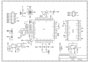
The GSM part is based on SIM900D GSM module. SIM300DZ has the same pin layout and designation so it might be used as a replacement of SIM900D. Q1 transistor, R2, R3 and R4 resistors are used to drive LED1 ‘NET LIGHT’ which indicates module networking status. CONN4 is a SMT antenna connector. Q2 transistor and R8, R9 resistors facilitate module powering on and off via PWRK line. C4, C5, C6 capacitors, L2 and L3 inductors and CONN9 are optional for external microphone connection. Optional CONN3 connector is for debugging and firmware upgrade purposes. CONN7 SIM CARD holder is connected to the module through matching the impedance R5, R6 and R7 resistors and D1 for ESD protection. Optional CONN6 and CONN8 are for Li-Ion battery and battery charger accodingly. The modem is connected to the host controller via CONN1 connector with the following pin designations: TX, RX, RTS, CTS are used for serial communication, STAT is used to detect whether the module is switched on or off, PWRK is for the actuall switching on and off, RESG is used for Copernicus GPS module reset.
The GPS part is based on Copernicus module. It also has SMT connector CONN5 for GPS antenna and CONN2 for connection to the second serial port on a host controller.The module might be set to power down mode via STBY line.
There are a few options for powering the device. First of all, 3.4V DC 2A could be supplied through pins 8, 10 of CONN1. The typical voltage is usually 3.3 but it is just not enough for SIM900D, the critical level is 3.4V so if you have voltage of this level on your host controller then use this option. Just keep in mind that SIM900D peak current consuption is 2A. In this case the power selector JP1, JP2 should be shorted with jumpers at 1-2 pins. The second option is to use 12V external voltage then U3 regulator, C2, C3, D2, L1, R10, R11 and FB1 elements should be soldered. It provides SIM900D with optimum 3.7V. In this case 1-2 pins of JP3 and 2-3 of JP1, JP2 must be closed with jumpers. Now there is still a need in 3.3V for the GPS chip, it could be supplied via pin 6 of CONN2 connector or provided by soldering U4, C9, L4 and C10 components, it will give 3.3V at 150 mA which could be used somewhere else. In the latter case the only required input voltage to be provided externally will be 12V.
The project’s circuit diagram is given below:
Note:Circuit diagrams are licensed under a Creative Commons Attribution Share-Alike license,which allows for both personal and commercial derivative works,as long as they credit ‘AVR Magictale Projects’ and release their designs under the same license.


Leave a Reply
You must be logged in to post a comment.