


Having hardware and software configurable platform gives the ultimate flexibility. Having FPGA fabric and two ARM cores integrated into a single System-On-Chip (SoC) gives benefits of the two (hardware and software) worlds, compact size, advanced optimisation of such integration, reduces the time for development effort, simplifies subsequent testing, verification and validation. Today we are reviewing a great development platform with Zynq 7020 SoC from Xilinx. Let’s implement an equivalent of ‘Hello World’ application, in our case we are going to create 6 independent PWM channels in hardware, connect them to the two RGB LEDs and write a simple demo cycling through the colours.
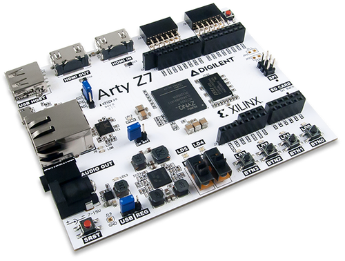
The board that we are going to use is Arty Z7-20, its picture is given below:
We will also need a Vivado Webpack SDK, we will be using relatively old but stable revision 2017.3 but our readers have a full freedom of using something more recent. At the end of the day, the tool doesn’t matter as much as the actual engineer who uses the tool.
Let’s iterate through the steps of our activities. We are going to create a blank Vivado project, create a board design, design a new AXI IP core which will control our PWM channels through the set of registers, go back to the main project, create a Zynq processing system, enable board’s system clock and RGB LED peripheral and connect it to the processing system through our newly designed PWM IP Core. Then add constraints, generate HDL wrapper, synthesize and run the implementation, generate bitstream and hardware description, export it to SDK, create an empty FreeRTOS application, write our C code for controlling LEDs and then run the demo.
There is not so much of the code writing during this exercise, it is customising VHDL template for the AXI IP Core and C-code. Let’s start by looking at the VHDL code.
First code example is given below, it is autogenerated led_pwm_v1_0.vhd that acts as a wrapper around the AXI Bus Interface. The highlighted lines are our customised additions to the autogenerated code:
library ieee;
use ieee.std_logic_1164.all;
use ieee.numeric_std.all;

entity led_pwm_v1_0 is
	generic (
		-- Users to add parameters here

		-- User parameters ends
		-- Do not modify the parameters beyond this line


		-- Parameters of Axi Slave Bus Interface S00_AXI
		C_S00_AXI_DATA_WIDTH	: integer	:= 32;
		C_S00_AXI_ADDR_WIDTH	: integer	:= 5
	);
	port (
		-- Users to add ports here
		gpio_io_o : out std_logic_vector(5 downto 0);
		-- User ports ends
		-- Do not modify the ports beyond this line


		-- Ports of Axi Slave Bus Interface S00_AXI
		s00_axi_aclk	: in std_logic;
		s00_axi_aresetn	: in std_logic;
		s00_axi_awaddr	: in std_logic_vector(C_S00_AXI_ADDR_WIDTH-1 downto 0);
		s00_axi_awprot	: in std_logic_vector(2 downto 0);
		s00_axi_awvalid	: in std_logic;
		s00_axi_awready	: out std_logic;
		s00_axi_wdata	: in std_logic_vector(C_S00_AXI_DATA_WIDTH-1 downto 0);
		s00_axi_wstrb	: in std_logic_vector((C_S00_AXI_DATA_WIDTH/8)-1 downto 0);
		s00_axi_wvalid	: in std_logic;
		s00_axi_wready	: out std_logic;
		s00_axi_bresp	: out std_logic_vector(1 downto 0);
		s00_axi_bvalid	: out std_logic;
		s00_axi_bready	: in std_logic;
		s00_axi_araddr	: in std_logic_vector(C_S00_AXI_ADDR_WIDTH-1 downto 0);
		s00_axi_arprot	: in std_logic_vector(2 downto 0);
		s00_axi_arvalid	: in std_logic;
		s00_axi_arready	: out std_logic;
		s00_axi_rdata	: out std_logic_vector(C_S00_AXI_DATA_WIDTH-1 downto 0);
		s00_axi_rresp	: out std_logic_vector(1 downto 0);
		s00_axi_rvalid	: out std_logic;
		s00_axi_rready	: in std_logic
	);
end led_pwm_v1_0;

architecture arch_imp of led_pwm_v1_0 is

	-- component declaration
	component led_pwm_v1_0_S00_AXI is
		generic (
		C_S_AXI_DATA_WIDTH	: integer	:= 32;
		C_S_AXI_ADDR_WIDTH	: integer	:= 5
		);
		port (
		rgb_led_tri_o : out std_logic_vector(5 downto 0);
		S_AXI_ACLK	: in std_logic;
		S_AXI_ARESETN	: in std_logic;
		S_AXI_AWADDR	: in std_logic_vector(C_S_AXI_ADDR_WIDTH-1 downto 0);
		S_AXI_AWPROT	: in std_logic_vector(2 downto 0);
		S_AXI_AWVALID	: in std_logic;
		S_AXI_AWREADY	: out std_logic;
		S_AXI_WDATA	: in std_logic_vector(C_S_AXI_DATA_WIDTH-1 downto 0);
		S_AXI_WSTRB	: in std_logic_vector((C_S_AXI_DATA_WIDTH/8)-1 downto 0);
		S_AXI_WVALID	: in std_logic;
		S_AXI_WREADY	: out std_logic;
		S_AXI_BRESP	: out std_logic_vector(1 downto 0);
		S_AXI_BVALID	: out std_logic;
		S_AXI_BREADY	: in std_logic;
		S_AXI_ARADDR	: in std_logic_vector(C_S_AXI_ADDR_WIDTH-1 downto 0);
		S_AXI_ARPROT	: in std_logic_vector(2 downto 0);
		S_AXI_ARVALID	: in std_logic;
		S_AXI_ARREADY	: out std_logic;
		S_AXI_RDATA	: out std_logic_vector(C_S_AXI_DATA_WIDTH-1 downto 0);
		S_AXI_RRESP	: out std_logic_vector(1 downto 0);
		S_AXI_RVALID	: out std_logic;
		S_AXI_RREADY	: in std_logic
		);
	end component led_pwm_v1_0_S00_AXI;

begin

-- Instantiation of Axi Bus Interface S00_AXI
led_pwm_v1_0_S00_AXI_inst : led_pwm_v1_0_S00_AXI
	generic map (
		C_S_AXI_DATA_WIDTH	=> C_S00_AXI_DATA_WIDTH,
		C_S_AXI_ADDR_WIDTH	=> C_S00_AXI_ADDR_WIDTH
	)
	port map (
		rgb_led_tri_o => gpio_io_o,
		S_AXI_ACLK	=> s00_axi_aclk,
		S_AXI_ARESETN	=> s00_axi_aresetn,
		S_AXI_AWADDR	=> s00_axi_awaddr,
		S_AXI_AWPROT	=> s00_axi_awprot,
		S_AXI_AWVALID	=> s00_axi_awvalid,
		S_AXI_AWREADY	=> s00_axi_awready,
		S_AXI_WDATA	=> s00_axi_wdata,
		S_AXI_WSTRB	=> s00_axi_wstrb,
		S_AXI_WVALID	=> s00_axi_wvalid,
		S_AXI_WREADY	=> s00_axi_wready,
		S_AXI_BRESP	=> s00_axi_bresp,
		S_AXI_BVALID	=> s00_axi_bvalid,
		S_AXI_BREADY	=> s00_axi_bready,
		S_AXI_ARADDR	=> s00_axi_araddr,
		S_AXI_ARPROT	=> s00_axi_arprot,
		S_AXI_ARVALID	=> s00_axi_arvalid,
		S_AXI_ARREADY	=> s00_axi_arready,
		S_AXI_RDATA	=> s00_axi_rdata,
		S_AXI_RRESP	=> s00_axi_rresp,
		S_AXI_RVALID	=> s00_axi_rvalid,
		S_AXI_RREADY	=> s00_axi_rready
	);

	-- Add user logic here

	-- User logic ends

end arch_imp;
Second code example is autogenerated led_pwm_ip_v3_0_S00_AXI.vhd which is the actual the AXI Bus Interface. Once again, the highlighted lines are manual additions to the autogenerated code. The code is modified to give more meaningful names to the four slave registers accessible through the ARM CPU, these are the code and the registers:
library ieee;
use ieee.std_logic_1164.all;
use ieee.numeric_std.all;

entity led_pwm_v1_0_S00_AXI is
	generic (
		-- Users to add parameters here

		-- User parameters ends
		-- Do not modify the parameters beyond this line

		-- Width of S_AXI data bus
		C_S_AXI_DATA_WIDTH	: integer	:= 32;
		-- Width of S_AXI address bus
		C_S_AXI_ADDR_WIDTH	: integer	:= 5
	);
	port (
		-- Users to add ports here
		rgb_led_tri_o : out std_logic_vector(5 downto 0);
		-- User ports ends
		-- Do not modify the ports beyond this line

		-- Global Clock Signal
		S_AXI_ACLK	: in std_logic;
		-- Global Reset Signal. This Signal is Active LOW
		S_AXI_ARESETN	: in std_logic;
		-- Write address (issued by master, acceped by Slave)
		S_AXI_AWADDR	: in std_logic_vector(C_S_AXI_ADDR_WIDTH-1 downto 0);
		-- Write channel Protection type. This signal indicates the
    		-- privilege and security level of the transaction, and whether
    		-- the transaction is a data access or an instruction access.
		S_AXI_AWPROT	: in std_logic_vector(2 downto 0);
		-- Write address valid. This signal indicates that the master signaling
    		-- valid write address and control information.
		S_AXI_AWVALID	: in std_logic;
		-- Write address ready. This signal indicates that the slave is ready
    		-- to accept an address and associated control signals.
		S_AXI_AWREADY	: out std_logic;
		-- Write data (issued by master, acceped by Slave)
		S_AXI_WDATA	: in std_logic_vector(C_S_AXI_DATA_WIDTH-1 downto 0);
		-- Write strobes. This signal indicates which byte lanes hold
    		-- valid data. There is one write strobe bit for each eight
    		-- bits of the write data bus.
		S_AXI_WSTRB	: in std_logic_vector((C_S_AXI_DATA_WIDTH/8)-1 downto 0);
		-- Write valid. This signal indicates that valid write
    		-- data and strobes are available.
		S_AXI_WVALID	: in std_logic;
		-- Write ready. This signal indicates that the slave
    		-- can accept the write data.
		S_AXI_WREADY	: out std_logic;
		-- Write response. This signal indicates the status
    		-- of the write transaction.
		S_AXI_BRESP	: out std_logic_vector(1 downto 0);
		-- Write response valid. This signal indicates that the channel
    		-- is signaling a valid write response.
		S_AXI_BVALID	: out std_logic;
		-- Response ready. This signal indicates that the master
    		-- can accept a write response.
		S_AXI_BREADY	: in std_logic;
		-- Read address (issued by master, acceped by Slave)
		S_AXI_ARADDR	: in std_logic_vector(C_S_AXI_ADDR_WIDTH-1 downto 0);
		-- Protection type. This signal indicates the privilege
    		-- and security level of the transaction, and whether the
    		-- transaction is a data access or an instruction access.
		S_AXI_ARPROT	: in std_logic_vector(2 downto 0);
		-- Read address valid. This signal indicates that the channel
    		-- is signaling valid read address and control information.
		S_AXI_ARVALID	: in std_logic;
		-- Read address ready. This signal indicates that the slave is
    		-- ready to accept an address and associated control signals.
		S_AXI_ARREADY	: out std_logic;
		-- Read data (issued by slave)
		S_AXI_RDATA	: out std_logic_vector(C_S_AXI_DATA_WIDTH-1 downto 0);
		-- Read response. This signal indicates the status of the
    		-- read transfer.
		S_AXI_RRESP	: out std_logic_vector(1 downto 0);
		-- Read valid. This signal indicates that the channel is
    		-- signaling the required read data.
		S_AXI_RVALID	: out std_logic;
		-- Read ready. This signal indicates that the master can
    		-- accept the read data and response information.
		S_AXI_RREADY	: in std_logic
	);
end led_pwm_v1_0_S00_AXI;

architecture arch_imp of led_pwm_v1_0_S00_AXI is

        component pwm is
            generic (
               G_DATA_WIDTH : integer := 32);
            port (
                f_aclk : in std_logic;
                i_aresetn : in std_logic;
                i_pwm_module : in std_logic_vector(C_S_AXI_DATA_WIDTH - 1 downto 0);
                i_pwm_width : in std_logic_vector(C_S_AXI_DATA_WIDTH - 1 downto 0);
                o_pwm : out std_logic);
        end component;

	-- AXI4LITE signals
	signal axi_awaddr	: std_logic_vector(C_S_AXI_ADDR_WIDTH-1 downto 0);
	signal axi_awready	: std_logic;
	signal axi_wready	: std_logic;
	signal axi_bresp	: std_logic_vector(1 downto 0);
	signal axi_bvalid	: std_logic;
	signal axi_araddr	: std_logic_vector(C_S_AXI_ADDR_WIDTH-1 downto 0);
	signal axi_arready	: std_logic;
	signal axi_rdata	: std_logic_vector(C_S_AXI_DATA_WIDTH-1 downto 0);
	signal axi_rresp	: std_logic_vector(1 downto 0);
	signal axi_rvalid	: std_logic;

	-- Example-specific design signals
	-- local parameter for addressing 32 bit / 64 bit C_S_AXI_DATA_WIDTH
	-- ADDR_LSB is used for addressing 32/64 bit registers/memories
	-- ADDR_LSB = 2 for 32 bits (n downto 2)
	-- ADDR_LSB = 3 for 64 bits (n downto 3)
	constant ADDR_LSB  : integer := (C_S_AXI_DATA_WIDTH/32)+ 1;
	constant OPT_MEM_ADDR_BITS : integer := 2;
	------------------------------------------------
	---- Signals for user logic register space example
	--------------------------------------------------
	---- Number of Slave Registers 7
        signal i_pwm_module :std_logic_vector(C_S_AXI_DATA_WIDTH-1 downto 0);
        signal i_pwm_width0 :std_logic_vector(C_S_AXI_DATA_WIDTH-1 downto 0);
        signal i_pwm_width1 :std_logic_vector(C_S_AXI_DATA_WIDTH-1 downto 0);
        signal i_pwm_width2 :std_logic_vector(C_S_AXI_DATA_WIDTH-1 downto 0);
        signal i_pwm_width3 :std_logic_vector(C_S_AXI_DATA_WIDTH-1 downto 0);
        signal i_pwm_width4 :std_logic_vector(C_S_AXI_DATA_WIDTH-1 downto 0);
        signal i_pwm_width5 :std_logic_vector(C_S_AXI_DATA_WIDTH-1 downto 0);
	signal slv_reg_rden	: std_logic;
	signal slv_reg_wren	: std_logic;
	signal reg_data_out	:std_logic_vector(C_S_AXI_DATA_WIDTH-1 downto 0);
	signal byte_index	: integer;
	signal aw_en	: std_logic;

begin

        pwm1: pwm
            generic map (
                G_DATA_WIDTH => C_S_AXI_DATA_WIDTH
            )
            port map (
                f_aclk => S_AXI_ACLK,
                i_aresetn => S_AXI_ARESETN,
                i_pwm_module => i_pwm_module,
                i_pwm_width => i_pwm_width0,
                o_pwm => rgb_led_tri_o(0)
            );

        pwm2: pwm
            generic map (
                G_DATA_WIDTH => C_S_AXI_DATA_WIDTH
            )
            port map (
                f_aclk => S_AXI_ACLK,
                i_aresetn => S_AXI_ARESETN,
                i_pwm_module => i_pwm_module,
                i_pwm_width => i_pwm_width1,
                o_pwm => rgb_led_tri_o(1)
            );

        pwm3: pwm
            generic map (
                G_DATA_WIDTH => C_S_AXI_DATA_WIDTH
            )
            port map (
                f_aclk => S_AXI_ACLK,
                i_aresetn => S_AXI_ARESETN,
                i_pwm_module => i_pwm_module,
                i_pwm_width => i_pwm_width2,
                o_pwm => rgb_led_tri_o(2)
            );

        pwm4: pwm
            generic map (
                G_DATA_WIDTH => C_S_AXI_DATA_WIDTH
            )
            port map (
                f_aclk => S_AXI_ACLK,
                i_aresetn => S_AXI_ARESETN,
                i_pwm_module => i_pwm_module,
                i_pwm_width => i_pwm_width3,
                o_pwm => rgb_led_tri_o(3)
            );

        pwm5: pwm
            generic map (
                G_DATA_WIDTH => C_S_AXI_DATA_WIDTH
            )
            port map (
                f_aclk => S_AXI_ACLK,
                i_aresetn => S_AXI_ARESETN,
                i_pwm_module => i_pwm_module,
                i_pwm_width => i_pwm_width4,
                o_pwm => rgb_led_tri_o(4)
            );

        pwm6: pwm
            generic map (
                G_DATA_WIDTH => C_S_AXI_DATA_WIDTH
            )
            port map (
                f_aclk => S_AXI_ACLK,
                i_aresetn => S_AXI_ARESETN,
                i_pwm_module => i_pwm_module,
                i_pwm_width => i_pwm_width5,
                o_pwm => rgb_led_tri_o(5)
            );

	-- I/O Connections assignments

	S_AXI_AWREADY	<= axi_awready;
	S_AXI_WREADY	<= axi_wready;
	S_AXI_BRESP	<= axi_bresp;
	S_AXI_BVALID	<= axi_bvalid;
	S_AXI_ARREADY	<= axi_arready;
	S_AXI_RDATA	<= axi_rdata;
	S_AXI_RRESP	<= axi_rresp;
	S_AXI_RVALID	<= axi_rvalid;
	-- Implement axi_awready generation
	-- axi_awready is asserted for one S_AXI_ACLK clock cycle when both
	-- S_AXI_AWVALID and S_AXI_WVALID are asserted. axi_awready is
	-- de-asserted when reset is low.

	process (S_AXI_ACLK)
	begin
	  if rising_edge(S_AXI_ACLK) then
	    if S_AXI_ARESETN = '0' then
	      axi_awready <= '0';
	      aw_en <= '1';
	    else
	      if (axi_awready = '0' and S_AXI_AWVALID = '1' and S_AXI_WVALID = '1' and aw_en = '1') then
	        -- slave is ready to accept write address when
	        -- there is a valid write address and write data
	        -- on the write address and data bus. This design
	        -- expects no outstanding transactions.
	        axi_awready <= '1';
	        elsif (S_AXI_BREADY = '1' and axi_bvalid = '1') then
	            aw_en <= '1';
	        	axi_awready <= '0';
	      else
	        axi_awready <= '0';
	      end if;
	    end if;
	  end if;
	end process;

	-- Implement axi_awaddr latching
	-- This process is used to latch the address when both
	-- S_AXI_AWVALID and S_AXI_WVALID are valid.

	process (S_AXI_ACLK)
	begin
	  if rising_edge(S_AXI_ACLK) then
	    if S_AXI_ARESETN = '0' then
	      axi_awaddr <= (others => '0');
	    else
	      if (axi_awready = '0' and S_AXI_AWVALID = '1' and S_AXI_WVALID = '1' and aw_en = '1') then
	        -- Write Address latching
	        axi_awaddr <= S_AXI_AWADDR;
	      end if;
	    end if;
	  end if;
	end process;

	-- Implement axi_wready generation
	-- axi_wready is asserted for one S_AXI_ACLK clock cycle when both
	-- S_AXI_AWVALID and S_AXI_WVALID are asserted. axi_wready is
	-- de-asserted when reset is low.

	process (S_AXI_ACLK)
	begin
	  if rising_edge(S_AXI_ACLK) then
	    if S_AXI_ARESETN = '0' then
	      axi_wready <= '0';
	    else
	      if (axi_wready = '0' and S_AXI_WVALID = '1' and S_AXI_AWVALID = '1' and aw_en = '1') then
	          -- slave is ready to accept write data when
	          -- there is a valid write address and write data
	          -- on the write address and data bus. This design
	          -- expects no outstanding transactions.
	          axi_wready <= '1';
	      else
	        axi_wready <= '0';
	      end if;
	    end if;
	  end if;
	end process;

	-- Implement memory mapped register select and write logic generation
	-- The write data is accepted and written to memory mapped registers when
	-- axi_awready, S_AXI_WVALID, axi_wready and S_AXI_WVALID are asserted. Write strobes are used to
	-- select byte enables of slave registers while writing.
	-- These registers are cleared when reset (active low) is applied.
	-- Slave register write enable is asserted when valid address and data are available
	-- and the slave is ready to accept the write address and write data.
	slv_reg_wren <= axi_wready and S_AXI_WVALID and axi_awready and S_AXI_AWVALID ;

	process (S_AXI_ACLK)
	variable loc_addr :std_logic_vector(OPT_MEM_ADDR_BITS downto 0);
	begin
	  if rising_edge(S_AXI_ACLK) then
	    if S_AXI_ARESETN = '0' then
                i_pwm_module <= (others => '0');
                i_pwm_width0 <= (others => '0');
                i_pwm_width1 <= (others => '0');
                i_pwm_width2 <= (others => '0');
                i_pwm_width3 <= (others => '0');
                i_pwm_width4 <= (others => '0');
                i_pwm_width5 <= (others => '0');
	    else
	      loc_addr := axi_awaddr(ADDR_LSB + OPT_MEM_ADDR_BITS downto ADDR_LSB);
	      if (slv_reg_wren = '1') then
	        case loc_addr is
	          when b"000" =>
	            for byte_index in 0 to (C_S_AXI_DATA_WIDTH/8-1) loop
	              if ( S_AXI_WSTRB(byte_index) = '1' ) then
	                -- Respective byte enables are asserted as per write strobes
	                -- slave registor 0
	                i_pwm_module(byte_index*8+7 downto byte_index*8) <= S_AXI_WDATA(byte_index*8+7 downto byte_index*8);
	              end if;
	            end loop;
	          when b"001" =>
	            for byte_index in 0 to (C_S_AXI_DATA_WIDTH/8-1) loop
	              if ( S_AXI_WSTRB(byte_index) = '1' ) then
	                -- Respective byte enables are asserted as per write strobes
	                -- slave registor 1
	                i_pwm_width0(byte_index*8+7 downto byte_index*8) <= S_AXI_WDATA(byte_index*8+7 downto byte_index*8);
	              end if;
	            end loop;
	          when b"010" =>
	            for byte_index in 0 to (C_S_AXI_DATA_WIDTH/8-1) loop
	              if ( S_AXI_WSTRB(byte_index) = '1' ) then
	                -- Respective byte enables are asserted as per write strobes
	                -- slave registor 2
	                i_pwm_width1(byte_index*8+7 downto byte_index*8) <= S_AXI_WDATA(byte_index*8+7 downto byte_index*8);
	              end if;
	            end loop;
	          when b"011" =>
	            for byte_index in 0 to (C_S_AXI_DATA_WIDTH/8-1) loop
	              if ( S_AXI_WSTRB(byte_index) = '1' ) then
	                -- Respective byte enables are asserted as per write strobes
	                -- slave registor 3
	                i_pwm_width2(byte_index*8+7 downto byte_index*8) <= S_AXI_WDATA(byte_index*8+7 downto byte_index*8);
	              end if;
	            end loop;
	          when b"100" =>
	            for byte_index in 0 to (C_S_AXI_DATA_WIDTH/8-1) loop
	              if ( S_AXI_WSTRB(byte_index) = '1' ) then
	                -- Respective byte enables are asserted as per write strobes
	                -- slave registor 4
	                i_pwm_width3(byte_index*8+7 downto byte_index*8) <= S_AXI_WDATA(byte_index*8+7 downto byte_index*8);
	              end if;
	            end loop;
	          when b"101" =>
	            for byte_index in 0 to (C_S_AXI_DATA_WIDTH/8-1) loop
	              if ( S_AXI_WSTRB(byte_index) = '1' ) then
	                -- Respective byte enables are asserted as per write strobes
	                -- slave registor 5
	                i_pwm_width4(byte_index*8+7 downto byte_index*8) <= S_AXI_WDATA(byte_index*8+7 downto byte_index*8);
	              end if;
	            end loop;
	          when b"110" =>
	            for byte_index in 0 to (C_S_AXI_DATA_WIDTH/8-1) loop
	              if ( S_AXI_WSTRB(byte_index) = '1' ) then
	                -- Respective byte enables are asserted as per write strobes
	                -- slave registor 6
	                i_pwm_width5(byte_index*8+7 downto byte_index*8) <= S_AXI_WDATA(byte_index*8+7 downto byte_index*8);
	              end if;
	            end loop;
	          when others =>
	            i_pwm_module <= i_pwm_module;
	            i_pwm_width0 <= i_pwm_width0;
	            i_pwm_width1 <= i_pwm_width1;
	            i_pwm_width2 <= i_pwm_width2;
	            i_pwm_width3 <= i_pwm_width3;
	            i_pwm_width4 <= i_pwm_width4;
	            i_pwm_width5 <= i_pwm_width5;
	        end case;
	      end if;
	    end if;
	  end if;
	end process;

	-- Implement write response logic generation
	-- The write response and response valid signals are asserted by the slave
	-- when axi_wready, S_AXI_WVALID, axi_wready and S_AXI_WVALID are asserted.
	-- This marks the acceptance of address and indicates the status of
	-- write transaction.

	process (S_AXI_ACLK)
	begin
	  if rising_edge(S_AXI_ACLK) then
	    if S_AXI_ARESETN = '0' then
	      axi_bvalid  <= '0';
	      axi_bresp   <= "00"; --need to work more on the responses
	    else
	      if (axi_awready = '1' and S_AXI_AWVALID = '1' and axi_wready = '1' and S_AXI_WVALID = '1' and axi_bvalid = '0'  ) then
	        axi_bvalid <= '1';
	        axi_bresp  <= "00";
	      elsif (S_AXI_BREADY = '1' and axi_bvalid = '1') then   --check if bready is asserted while bvalid is high)
	        axi_bvalid <= '0';                                 -- (there is a possibility that bready is always asserted high)
	      end if;
	    end if;
	  end if;
	end process;

	-- Implement axi_arready generation
	-- axi_arready is asserted for one S_AXI_ACLK clock cycle when
	-- S_AXI_ARVALID is asserted. axi_awready is
	-- de-asserted when reset (active low) is asserted.
	-- The read address is also latched when S_AXI_ARVALID is
	-- asserted. axi_araddr is reset to zero on reset assertion.

	process (S_AXI_ACLK)
	begin
	  if rising_edge(S_AXI_ACLK) then
	    if S_AXI_ARESETN = '0' then
	      axi_arready <= '0';
	      axi_araddr  <= (others => '1');
	    else
	      if (axi_arready = '0' and S_AXI_ARVALID = '1') then
	        -- indicates that the slave has acceped the valid read address
	        axi_arready <= '1';
	        -- Read Address latching
	        axi_araddr  <= S_AXI_ARADDR;
	      else
	        axi_arready <= '0';
	      end if;
	    end if;
	  end if;
	end process;

	-- Implement axi_arvalid generation
	-- axi_rvalid is asserted for one S_AXI_ACLK clock cycle when both
	-- S_AXI_ARVALID and axi_arready are asserted. The slave registers
	-- data are available on the axi_rdata bus at this instance. The
	-- assertion of axi_rvalid marks the validity of read data on the
	-- bus and axi_rresp indicates the status of read transaction.axi_rvalid
	-- is deasserted on reset (active low). axi_rresp and axi_rdata are
	-- cleared to zero on reset (active low).
	process (S_AXI_ACLK)
	begin
	  if rising_edge(S_AXI_ACLK) then
	    if S_AXI_ARESETN = '0' then
	      axi_rvalid <= '0';
	      axi_rresp  <= "00";
	    else
	      if (axi_arready = '1' and S_AXI_ARVALID = '1' and axi_rvalid = '0') then
	        -- Valid read data is available at the read data bus
	        axi_rvalid <= '1';
	        axi_rresp  <= "00"; -- 'OKAY' response
	      elsif (axi_rvalid = '1' and S_AXI_RREADY = '1') then
	        -- Read data is accepted by the master
	        axi_rvalid <= '0';
	      end if;
	    end if;
	  end if;
	end process;

	-- Implement memory mapped register select and read logic generation
	-- Slave register read enable is asserted when valid address is available
	-- and the slave is ready to accept the read address.
	slv_reg_rden <= axi_arready and S_AXI_ARVALID and (not axi_rvalid) ;

	process (i_pwm_module, i_pwm_width0, i_pwm_width1, i_pwm_width2, i_pwm_width3, i_pwm_width4, i_pwm_width5, axi_araddr, S_AXI_ARESETN, slv_reg_rden)
	variable loc_addr :std_logic_vector(OPT_MEM_ADDR_BITS downto 0);
	begin
	    -- Address decoding for reading registers
	    loc_addr := axi_araddr(ADDR_LSB + OPT_MEM_ADDR_BITS downto ADDR_LSB);
	    case loc_addr is
	      when b"000" =>
	        reg_data_out <= i_pwm_module;
	      when b"001" =>
	        reg_data_out <= i_pwm_width0;
	      when b"010" =>
	        reg_data_out <= i_pwm_width1;
	      when b"011" =>
	        reg_data_out <= i_pwm_width2;
	      when b"100" =>
	        reg_data_out <= i_pwm_width3;
	      when b"101" =>
	        reg_data_out <= i_pwm_width4;
	      when b"110" =>
	        reg_data_out <= i_pwm_width5;
	      when others =>
	        reg_data_out  <= (others => '0');
	    end case;
	end process;

	-- Output register or memory read data
	process( S_AXI_ACLK ) is
	begin
	  if (rising_edge (S_AXI_ACLK)) then
	    if ( S_AXI_ARESETN = '0' ) then
	      axi_rdata  <= (others => '0');
	    else
	      if (slv_reg_rden = '1') then
	        -- When there is a valid read address (S_AXI_ARVALID) with
	        -- acceptance of read address by the slave (axi_arready),
	        -- output the read dada
	        -- Read address mux
	          axi_rdata <= reg_data_out;     -- register read data
	      end if;
	    end if;
	  end if;
	end process;


	-- Add user logic here

	-- User logic ends

end arch_imp;
| Register name | Number of dedicated bits | Description |
|---|---|---|
| i_pwm_module | C_S_AXI_DATA_WIDTH (32) | maximum value the PWM module counts to |
| Register name | Number of dedicated bits | Description |
|---|---|---|
| i_pwm_width0 | C_S_AXI_DATA_WIDTH (32) | maximum value of the counter when the PWM output is on for RED LED1 |
| i_pwm_width1 | C_S_AXI_DATA_WIDTH (32) | maximum value of the counter when the PWM output is on for GREEN LED1 |
| i_pwm_width2 | C_S_AXI_DATA_WIDTH (32) | maximum value of the counter when the PWM output is on for BLUE LED1 |
| Register name | Number of dedicated bits | Description |
|---|---|---|
| i_pwm_width3 | C_S_AXI_DATA_WIDTH (32) | maximum value of the counter when the PWM output is on for RED LED2 |
| i_pwm_width4 | C_S_AXI_DATA_WIDTH (32) | maximum value of the counter when the PWM output is on for GREEN LED2 |
| i_pwm_width5 | C_S_AXI_DATA_WIDTH (32) | maximum value of the counter when the PWM output is on for BLUE LED2 |
library ieee;
use ieee.std_logic_1164.all;
use ieee.numeric_std.all;

entity pwm is
  generic (
    G_DATA_WIDTH : integer := 32
  );
  port (
    -- Clock Signal
    f_aclk : in std_logic;
    -- Reset Signal. This Signal is Active LOW
    i_aresetn : in std_logic;
    i_pwm_module : in std_logic_vector(G_DATA_WIDTH - 1 downto 0);
    i_pwm_width : in std_logic_vector(G_DATA_WIDTH - 1 downto 0);
    -- The PWM-ed output
    o_pwm : out std_logic
  );
end pwm;

architecture arch_imp of pwm is

  signal s_max_count : unsigned(G_DATA_WIDTH - 1 downto 0);
  signal s_pwm_counter : unsigned(G_DATA_WIDTH - 1 downto 0);
  signal s_pwm_width : unsigned(G_DATA_WIDTH - 1 downto 0);
  signal s_tc_pwm_counter : std_logic;

begin
  s_tc_pwm_counter  <= '0' when(s_pwm_counter < s_max_count) else '1';  -- use to strobe new word

  p_state_out : process(f_aclk, i_aresetn)
  begin
    if (i_aresetn = '0') then
      s_max_count <= (others=>'0');
      s_pwm_width <= (others=>'0');
      s_pwm_counter <= (others=>'0');
      o_pwm <= '0';
    elsif (rising_edge(f_aclk)) then
      s_max_count <= unsigned(i_pwm_module);
      if (s_pwm_counter = 0) and (s_pwm_width /= s_max_count) then
        o_pwm <= '0';
      elsif (s_pwm_counter <= s_pwm_width) then
        o_pwm <= '1';
      else
        o_pwm <= '0';
      end if;

      if (s_tc_pwm_counter='1') then
        s_pwm_width <= unsigned(i_pwm_width);
      end if;

      if (s_pwm_counter = s_max_count) then
        s_pwm_counter <= to_unsigned(0, G_DATA_WIDTH);
      else
        s_pwm_counter <= s_pwm_counter + 1;
      end if;
    end if;
  end process p_state_out;
end arch_imp;
/*
 FreeRTOS based RGB PWM LED Demo for Arty Z7-20 board
 ====================================================

 This demo is a 'Hello World' application type running on
 Zynq FPGA chip from Xilinx and a starting point for
 doing Block design, IP Core creation, FreeRTOS application
 development, integration of PL and PS sides and packaging
 the whole project into a compact and elegant solution which
 sets a reference point for future projects.

 This project has a custom designed IP Core capable of
 driving 6 independent PWM channels which outputs are
 directly connected to the two RGB LEDs of the Arty board.

 Copyright (c) 2020 Dmitry Pakhomenko.
 dmitryp@magictale.com
 http://magictale.com

 This code is in the public domain.
*/

/* FreeRTOS includes. */
#include "FreeRTOS.h"
#include "task.h"
#include "timers.h"
/* Xilinx includes. */
#include "xil_printf.h"
#include "xparameters.h"
#include "xil_io.h"

#define BTIMER_ID 1
#define GTIMER_ID 2
#define RTIMER_ID 3
#define DELAY_1_SECOND 1000UL
#define DELAY_30_MSECONDS 30UL
#define DELAY_40_MSECONDS 40UL
#define DELAY_50_MSECONDS 50UL

#define RGB_LED_PWM_BASE XPAR_LED_PWM_0_S00_AXI_BASEADDR
#define RGB_LED_PWM_MODULE_OFFSET 0
#define RGB_LED0_PWM_BLUE_WIDTH_OFFSET 1
#define RGB_LED0_PWM_GREEN_WIDTH_OFFSET 2
#define RGB_LED0_PWM_RED_WIDTH_OFFSET 3
#define RGB_LED1_PWM_BLUE_WIDTH_OFFSET 4
#define RGB_LED1_PWM_GREEN_WIDTH_OFFSET 5
#define RGB_LED1_PWM_RED_WIDTH_OFFSET 6

#define RGB_LED_OFFSET_MULTIPLIER 4
#define RGB_LED_MAX_DUTY_CYCLE 0x30
#define RGB_LED_PWM_MODULE 0x80
#define ITEGRATIONS_IN_RGB_MODE 10

typedef enum
{
    RED_MODE = 0,
    GREEN_MODE,
    BLUE_MODE,
    RGB_MODE,
    END_MODE
} Blinking_Mode_Enum;

typedef struct
{
    uint8_t id;
    uint8_t duty_cycle;
    uint8_t intensity_ascending;
    uint8_t register_offset;
    TimerHandle_t xTimer;
} LED_Descriptor_Struct;

typedef struct
{
    LED_Descriptor_Struct leds[3];
    Blinking_Mode_Enum blinking_mode;
    uint8_t iterations_in_rgb_mode;
} RGB_LED_Descriptor_Struct;

static void prvLedCtrlTask(void *pvParameters);
static void vBlue0TimerCallback(TimerHandle_t pxTimer);
static void vGreen0TimerCallback(TimerHandle_t pxTimer);
static void vRed0TimerCallback(TimerHandle_t pxTimer);
static void vBlue1TimerCallback(TimerHandle_t pxTimer);
static void vGreen1TimerCallback(TimerHandle_t pxTimer);
static void vRed1TimerCallback(TimerHandle_t pxTimer);
static void vUpdateDutyCycle(RGB_LED_Descriptor_Struct * p_rgb_led_descriptor,
    LED_Descriptor_Struct * p_led_descriptor, uint8_t progress_mode);
static void progressBlinkingMode(RGB_LED_Descriptor_Struct * p_rgb_led_descriptor);

static TaskHandle_t xLedControlTask;
static RGB_LED_Descriptor_Struct rgb_led0 =
    {.leds =
        {
            {.id = RED_MODE, .duty_cycle = 0, .intensity_ascending = TRUE, .register_offset = RGB_LED0_PWM_RED_WIDTH_OFFSET, .xTimer = NULL},
            {.id = GREEN_MODE, .duty_cycle = 0, .intensity_ascending = TRUE, .register_offset = RGB_LED0_PWM_GREEN_WIDTH_OFFSET, .xTimer = NULL},
            {.id = BLUE_MODE, .duty_cycle = 0, .intensity_ascending = TRUE, .register_offset = RGB_LED0_PWM_BLUE_WIDTH_OFFSET, .xTimer = NULL}
        },
      .blinking_mode = RED_MODE,
      .iterations_in_rgb_mode = ITEGRATIONS_IN_RGB_MODE
    };

static RGB_LED_Descriptor_Struct rgb_led1 =
    {.leds =
        {
            {.id = RED_MODE, .duty_cycle = 0, .intensity_ascending = TRUE, .register_offset = RGB_LED1_PWM_RED_WIDTH_OFFSET, .xTimer = NULL},
            {.id = GREEN_MODE, .duty_cycle = 0, .intensity_ascending = TRUE, .register_offset = RGB_LED1_PWM_GREEN_WIDTH_OFFSET, .xTimer = NULL},
            {.id = BLUE_MODE, .duty_cycle = 0, .intensity_ascending = TRUE, .register_offset = RGB_LED1_PWM_BLUE_WIDTH_OFFSET, .xTimer = NULL}
        },
      .blinking_mode = RED_MODE,
      .iterations_in_rgb_mode = ITEGRATIONS_IN_RGB_MODE / 2
    };


int main(void)
{
    const TickType_t x30mseconds = pdMS_TO_TICKS(DELAY_30_MSECONDS);
    const TickType_t x40mseconds = pdMS_TO_TICKS(DELAY_40_MSECONDS);
    const TickType_t x50mseconds = pdMS_TO_TICKS(DELAY_50_MSECONDS);

    xil_printf("\r\n\r\nFreeRTOS version of RGB LED PWM Demo for Arty Z7-20 board\r\n");

    xTaskCreate(prvLedCtrlTask, /* The function that implements the task. */
                (const char*) "Led", /* Text name for the task, provided to assist debugging only. */
                configMINIMAL_STACK_SIZE, /* The stack allocated to the task. */
                NULL, /* The task parameter is not used, so set to NULL. */
                tskIDLE_PRIORITY, /* The task runs at the idle priority. */
                &xLedControlTask );

    //=== LED 0 ===
    rgb_led0.leds[BLUE_MODE].xTimer = xTimerCreate((const char *)"Blue0Timer",
                x30mseconds,
                pdFALSE,
                (void*)BTIMER_ID,
                vBlue0TimerCallback);
    /* Check the timer was created. */
    configASSERT(rgb_led0.leds[BLUE_MODE].xTimer);

    rgb_led0.leds[GREEN_MODE].xTimer = xTimerCreate((const char *)"Green0Timer",
                x40mseconds,
                pdFALSE,
                (void*)GTIMER_ID,
                vGreen0TimerCallback);
    /* Check the timer was created. */
    configASSERT(rgb_led0.leds[GREEN_MODE].xTimer);

    rgb_led0.leds[RED_MODE].xTimer = xTimerCreate((const char *)"Red0Timer",
                x50mseconds,
                pdFALSE,
                (void*)RTIMER_ID,
                vRed0TimerCallback);
    /* Check the timer was created. */
    configASSERT(rgb_led0.leds[RED_MODE].xTimer);

    //=== LED 1 ===
    rgb_led1.leds[BLUE_MODE].xTimer = xTimerCreate((const char *)"Blue1Timer",
                x30mseconds / 2,
                pdFALSE,
                (void*)BTIMER_ID,
                vBlue1TimerCallback);
    /* Check the timer was created. */
    configASSERT(rgb_led1.leds[BLUE_MODE].xTimer);

    rgb_led1.leds[GREEN_MODE].xTimer = xTimerCreate((const char *)"Green1Timer",
                x40mseconds / 2,
                pdFALSE,
                (void*)GTIMER_ID,
                vGreen1TimerCallback);
    /* Check the timer was created. */
    configASSERT(rgb_led1.leds[GREEN_MODE].xTimer);

    rgb_led1.leds[RED_MODE].xTimer = xTimerCreate((const char *)"Red1Timer",
                x50mseconds / 2,
                pdFALSE,
                (void*)RTIMER_ID,
                vRed1TimerCallback);
    /* Check the timer was created. */
    configASSERT(rgb_led0.leds[RED_MODE].xTimer);


    Xil_Out32(RGB_LED_PWM_BASE + RGB_LED_PWM_MODULE_OFFSET, RGB_LED_PWM_MODULE);

    /* start the timers with a block time of 0 ticks. This means as soon
       as the schedule starts the timers will start running and will expire after
       predefined number of milliseconds */
    xTimerStart(rgb_led0.leds[RED_MODE].xTimer, 0);
    xTimerStart(rgb_led0.leds[GREEN_MODE].xTimer, 0);
    xTimerStart(rgb_led0.leds[BLUE_MODE].xTimer, 0);

    xTimerStart(rgb_led1.leds[RED_MODE].xTimer, 0);
    xTimerStart(rgb_led1.leds[GREEN_MODE].xTimer, 0);
    xTimerStart(rgb_led1.leds[BLUE_MODE].xTimer, 0);

    /* Start the tasks and timer running. */
    vTaskStartScheduler();

    /* If all is well, the scheduler will now be running, and the following line
    will never be reached.  If the following line does execute, then there was
    insufficient FreeRTOS heap memory available for the idle and/or timer tasks
    to be created.  See the memory management section on the FreeRTOS web site
    for more details. */
    for(;;);
}

void progressBlinkingMode(RGB_LED_Descriptor_Struct * p_rgb_led_descriptor)
{
    if (p_rgb_led_descriptor->blinking_mode == RGB_MODE)
    {
        // In RGB mode we don't immediately progress to the next state but rather
        // loop for several cycles defined in iterations_in_rgb_mode
        if (p_rgb_led_descriptor->iterations_in_rgb_mode == 0)
        {
            p_rgb_led_descriptor->blinking_mode++;
        }
        else
        {
            p_rgb_led_descriptor->iterations_in_rgb_mode--;
        }
    }
    else
    {
        p_rgb_led_descriptor->blinking_mode++;
    }

    if (p_rgb_led_descriptor->blinking_mode >= END_MODE)
    {
        p_rgb_led_descriptor->blinking_mode = RED_MODE;

        Xil_Out32(RGB_LED_PWM_BASE + p_rgb_led_descriptor->leds[RED_MODE].register_offset * RGB_LED_OFFSET_MULTIPLIER, 0);
        Xil_Out32(RGB_LED_PWM_BASE + p_rgb_led_descriptor->leds[GREEN_MODE].register_offset * RGB_LED_OFFSET_MULTIPLIER, 0);
        Xil_Out32(RGB_LED_PWM_BASE + p_rgb_led_descriptor->leds[BLUE_MODE].register_offset * RGB_LED_OFFSET_MULTIPLIER, 0);

        p_rgb_led_descriptor->leds[RED_MODE].duty_cycle = 0;
        p_rgb_led_descriptor->leds[GREEN_MODE].duty_cycle = 0;
        p_rgb_led_descriptor->leds[BLUE_MODE].duty_cycle = 0;

        p_rgb_led_descriptor->leds[RED_MODE].intensity_ascending = TRUE;
        p_rgb_led_descriptor->leds[GREEN_MODE].intensity_ascending = TRUE;
        p_rgb_led_descriptor->leds[BLUE_MODE].intensity_ascending = TRUE;
        p_rgb_led_descriptor->iterations_in_rgb_mode = ITEGRATIONS_IN_RGB_MODE;
    }
}

static void prvLedCtrlTask(void *pvParameters)
{
    const TickType_t x1second = pdMS_TO_TICKS( DELAY_1_SECOND );
    for(;;)
    {
        /* Delay for 1 second. */
        vTaskDelay(x1second);
        // TODO: instead of just waiting for timers do something useful in main thread
    }
}

static void vUpdateDutyCycle(RGB_LED_Descriptor_Struct * p_rgb_led_descriptor,
    LED_Descriptor_Struct * p_led_descriptor, uint8_t progress_mode)
{
    UBaseType_t uxSavedInterruptStatus;
    uxSavedInterruptStatus = taskENTER_CRITICAL_FROM_ISR();

    if (
        (p_rgb_led_descriptor->blinking_mode == RGB_MODE) ||
        (p_rgb_led_descriptor->blinking_mode == RED_MODE && p_led_descriptor->id == RED_MODE) ||
        (p_rgb_led_descriptor->blinking_mode == BLUE_MODE && p_led_descriptor->id == BLUE_MODE) ||
        (p_rgb_led_descriptor->blinking_mode == GREEN_MODE && p_led_descriptor->id == GREEN_MODE)
        )
    {
        Xil_Out32(RGB_LED_PWM_BASE + p_led_descriptor->register_offset * RGB_LED_OFFSET_MULTIPLIER, p_led_descriptor->duty_cycle);


        if ( p_led_descriptor->intensity_ascending == TRUE )
        {
            p_led_descriptor->duty_cycle++;
            if (p_led_descriptor->duty_cycle >= RGB_LED_MAX_DUTY_CYCLE)
            {
                p_led_descriptor->intensity_ascending = FALSE;
            }
        }
        else
        {
            p_led_descriptor->duty_cycle--;
            if (p_led_descriptor->duty_cycle == 0)
            {
                p_led_descriptor->intensity_ascending = TRUE;
                if ((progress_mode == TRUE && p_rgb_led_descriptor->blinking_mode == RGB_MODE) ||
                     p_rgb_led_descriptor->blinking_mode == RED_MODE ||
                     p_rgb_led_descriptor->blinking_mode == BLUE_MODE ||
                     p_rgb_led_descriptor->blinking_mode == GREEN_MODE
                   )
                {
                    // In RGB mode we progress blinking mode only at the end of cycle of just one color
                    // in other modes we always progress
                    progressBlinkingMode(p_rgb_led_descriptor);
                }
            }
        }
    }

    taskEXIT_CRITICAL_FROM_ISR(uxSavedInterruptStatus);
}

//=== LED 0 ===
static void vBlue0TimerCallback(TimerHandle_t pxTimer)
{
    long lTimerId;
    configASSERT(pxTimer);
    lTimerId = (long)pvTimerGetTimerID(pxTimer);
    if (lTimerId != BTIMER_ID)
    {
        xil_printf("Blue 0 Timer failed\r\n");
    }
    vUpdateDutyCycle(&rgb_led0, &rgb_led0.leds[BLUE_MODE], TRUE);
    xTimerStart(rgb_led0.leds[BLUE_MODE].xTimer, 0);
}

static void vGreen0TimerCallback(TimerHandle_t pxTimer)
{
    long lTimerId;
    configASSERT(pxTimer);
    lTimerId = (long)pvTimerGetTimerID(pxTimer);
    if (lTimerId != GTIMER_ID)
    {
        xil_printf("Green 0 Timer failed\r\n");
    }
    vUpdateDutyCycle(&rgb_led0, &rgb_led0.leds[GREEN_MODE], FALSE);
    xTimerStart(rgb_led0.leds[GREEN_MODE].xTimer, 0);
}

static void vRed0TimerCallback(TimerHandle_t pxTimer)
{
    long lTimerId;
    configASSERT(pxTimer);
    lTimerId = (long)pvTimerGetTimerID(pxTimer);
    if (lTimerId != RTIMER_ID)
    {
        xil_printf("Red 0 Timer failed\r\n");
    }
    vUpdateDutyCycle(&rgb_led0, &rgb_led0.leds[RED_MODE], FALSE);
    xTimerStart(rgb_led0.leds[RED_MODE].xTimer, 0);
}

//=== LED 1 ===
static void vBlue1TimerCallback(TimerHandle_t pxTimer)
{
    long lTimerId;
    configASSERT(pxTimer);
    lTimerId = (long)pvTimerGetTimerID(pxTimer);
    if (lTimerId != BTIMER_ID)
    {
        xil_printf("Blue 1 Timer failed\r\n");
    }
    vUpdateDutyCycle(&rgb_led1, &rgb_led1.leds[BLUE_MODE], TRUE);
    xTimerStart(rgb_led1.leds[BLUE_MODE].xTimer, 0);
}

static void vGreen1TimerCallback(TimerHandle_t pxTimer)
{
    long lTimerId;
    configASSERT(pxTimer);
    lTimerId = (long)pvTimerGetTimerID(pxTimer);
    if (lTimerId != GTIMER_ID)
    {
        xil_printf("Green 1 Timer failed\r\n");
    }
    vUpdateDutyCycle(&rgb_led1, &rgb_led1.leds[GREEN_MODE], FALSE);
    xTimerStart(rgb_led1.leds[GREEN_MODE].xTimer, 0);
}

static void vRed1TimerCallback(TimerHandle_t pxTimer)
{
    long lTimerId;
    configASSERT(pxTimer);
    lTimerId = (long)pvTimerGetTimerID(pxTimer);
    if (lTimerId != RTIMER_ID)
    {
        xil_printf("Red 1 Timer failed\r\n");
    }
    vUpdateDutyCycle(&rgb_led1, &rgb_led1.leds[RED_MODE], FALSE);
    xTimerStart(rgb_led1.leds[RED_MODE].xTimer, 0);
}


Leave a Reply
You must be logged in to post a comment.