


Components are soldered on both sides of the PCB. Only components that need to provide the required functionality should be soldered. Depending on your situation, some components such as CONN1, CONN2, CONN4, CONN5, L1 etc can be soldered on either side of the board. There is no strict sequence for soldering but U1 should be probably installed first as it has many pins along three sides and should be positioned very precisely. The most challenging component to be soldered is D1 due to its smallest pin pitch (and which is actually used to protect SIM interface lines from ESD). If you can’t solder it then don’t do it – you will just need to take more ESD precautions when replacing SIM card.
PCB component layout for both sides is given below:

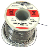
Time to begin soldering components. But before make sure that you have the following tools and materials get ready: solder iron with temperature control or soldering station, solder, solder wick, mutimeter, tweezers. We highly recommend to use solder paste in syringe packaging which will significantly improve the quality of your soldering. Based on our own experience we would advise to get SMD291NL that is available in Digikey.com, inexpensive and the the same time gives noticeable good results. To make things even more easier it would be also useful to have a magnifying glass and plenty of natural light (preferably daylight).
As many components are ESD sensitive it would be worth taking anti-static protection precautions. The tip would to be well earthed (grounded) in any circumstances when handling CMOS components, not only soldering them.
Leave a Reply
You must be logged in to post a comment.