


Building a 3D model from PCB design files can bring your project to a totally new level. It comes at a price as it requires extra design time but being properly done it saves a lot of effort and money in the future as it minimises risks by helping to capture issues on early stages of design cycle.
First and most obvious plus of a 3D model is that is allows to estimate dimensions and optimise component layout. This is especially useful when components are soldered on both sides of PCB and some components are located in close proximity to each other or even overlap if, for example, some passive elements are destined to be under a bigger one such as LCD/VFD display, sensor, heatsink or something else. Secondly, if a project comprises of a several PCBs it becomes even more important that there is no interference between them. Also 3D view helps to pick up such things as drill hole sizes as it becomes clear whether a pin fits in a hole or not. It is also useful to access the overall look of the future assembly before it is physically assembled and experiment with such things as PCB mask color for instance to make right choice. 3D design of PCBA is one step closer towards subsequent enclosure design, be it laser cut acrylic panels or a model for 3D printing. And finally, design files accompanied by a 3D model make a project to look very professional and significantly simplifying following creation of project’s documentation.
There is absolutely amazing plugin called EagleUp that makes a bridge between Eagle CAD and SketchUp. The plugin allows to automate export of PCB design files into 3D world but of course not everything can be automated – there is still need in 3D footprints that have to be created first. Some 3D footprints are already created by someone else and could be found at Google 3D Warehouse but be prepared that not all of them exist and you have to design a few models for your project by yourself. The whole process is thoroughly described here and here so we recommend to refer to these resources for more information. From our personal experience the only strange part that we found in EagleUp was a necessity to design footprints using meters instead of millimeters resulting the models to be 1000 times bigger. But this issue is easily rectified by scaling down fully modeled PCBA back to millimeters.
The result of our effort is given below as a model in Google 3D Warehouse.
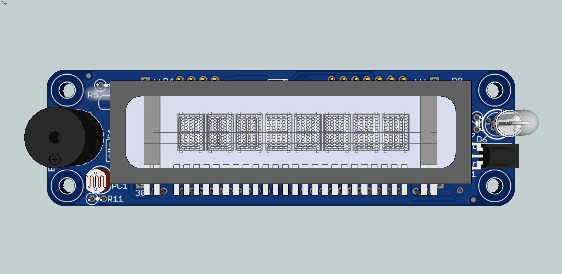
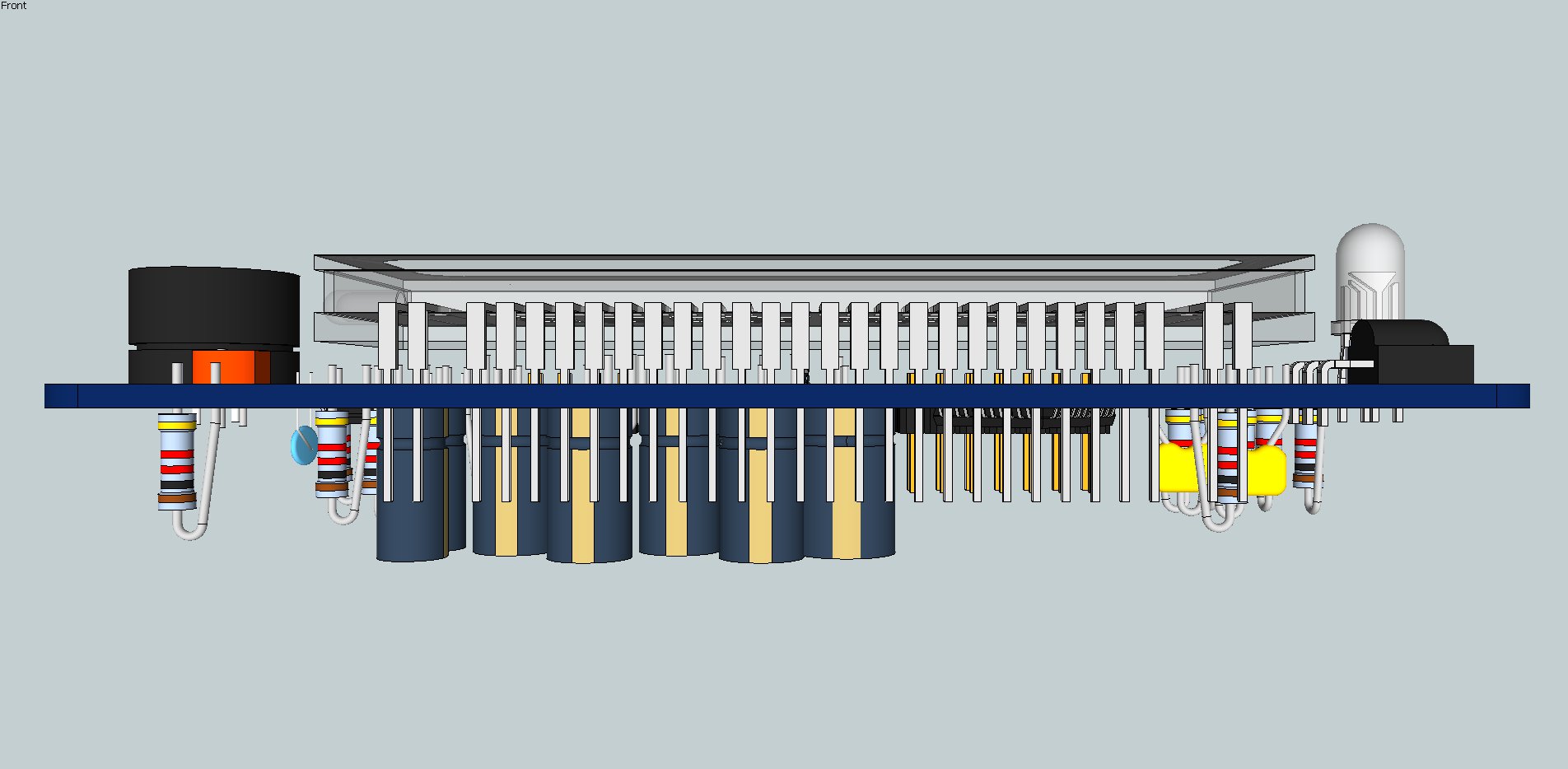
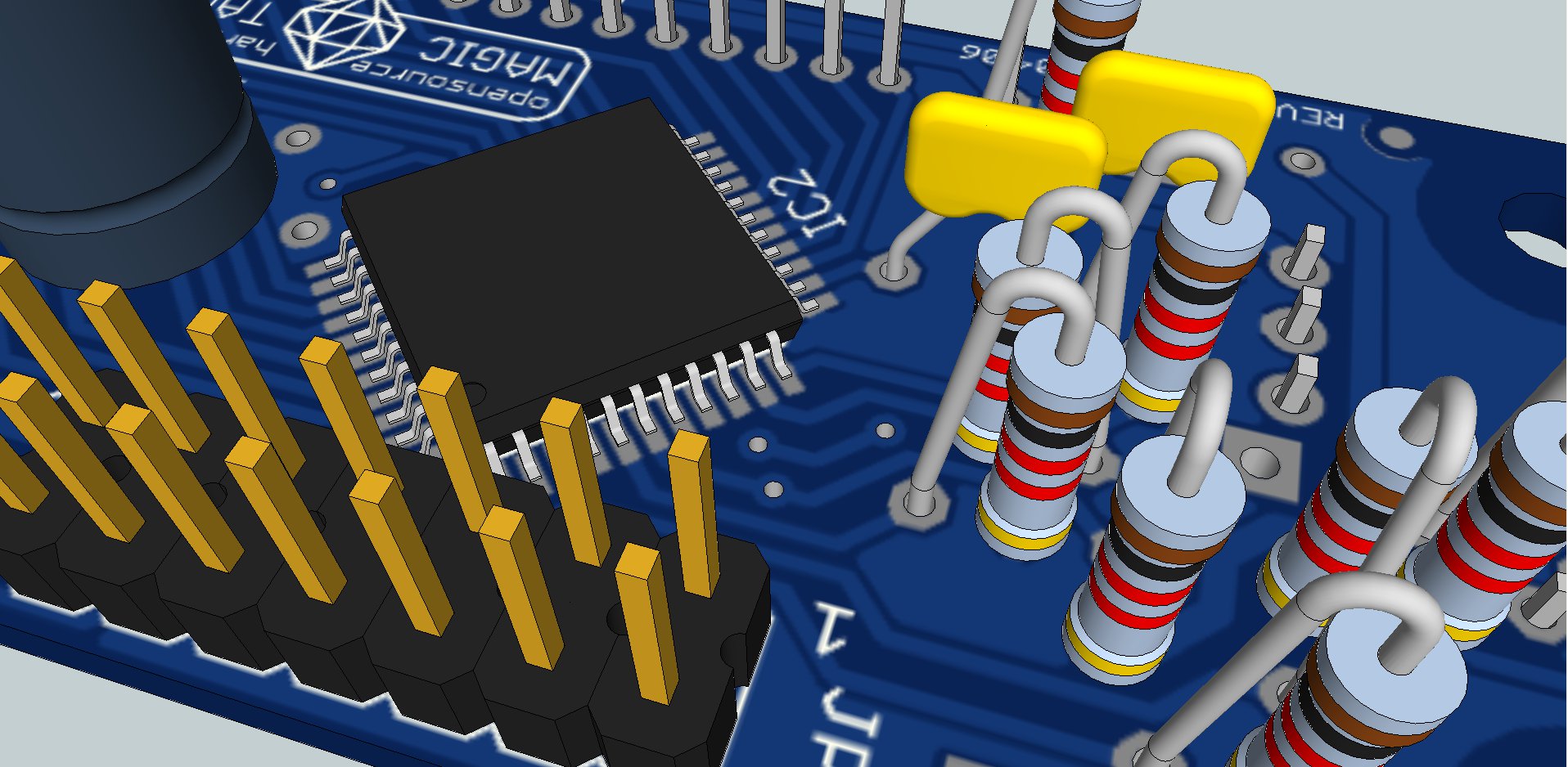
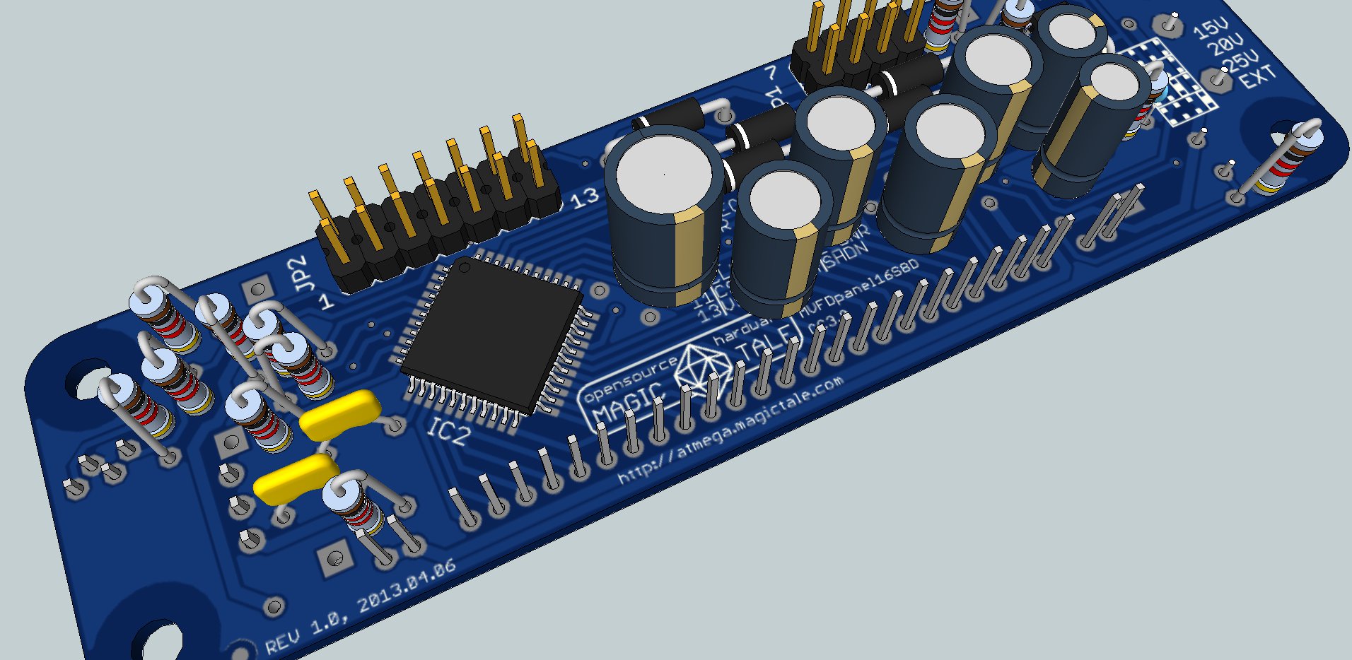
The pictures below show the model at different view angles in SketchUp.
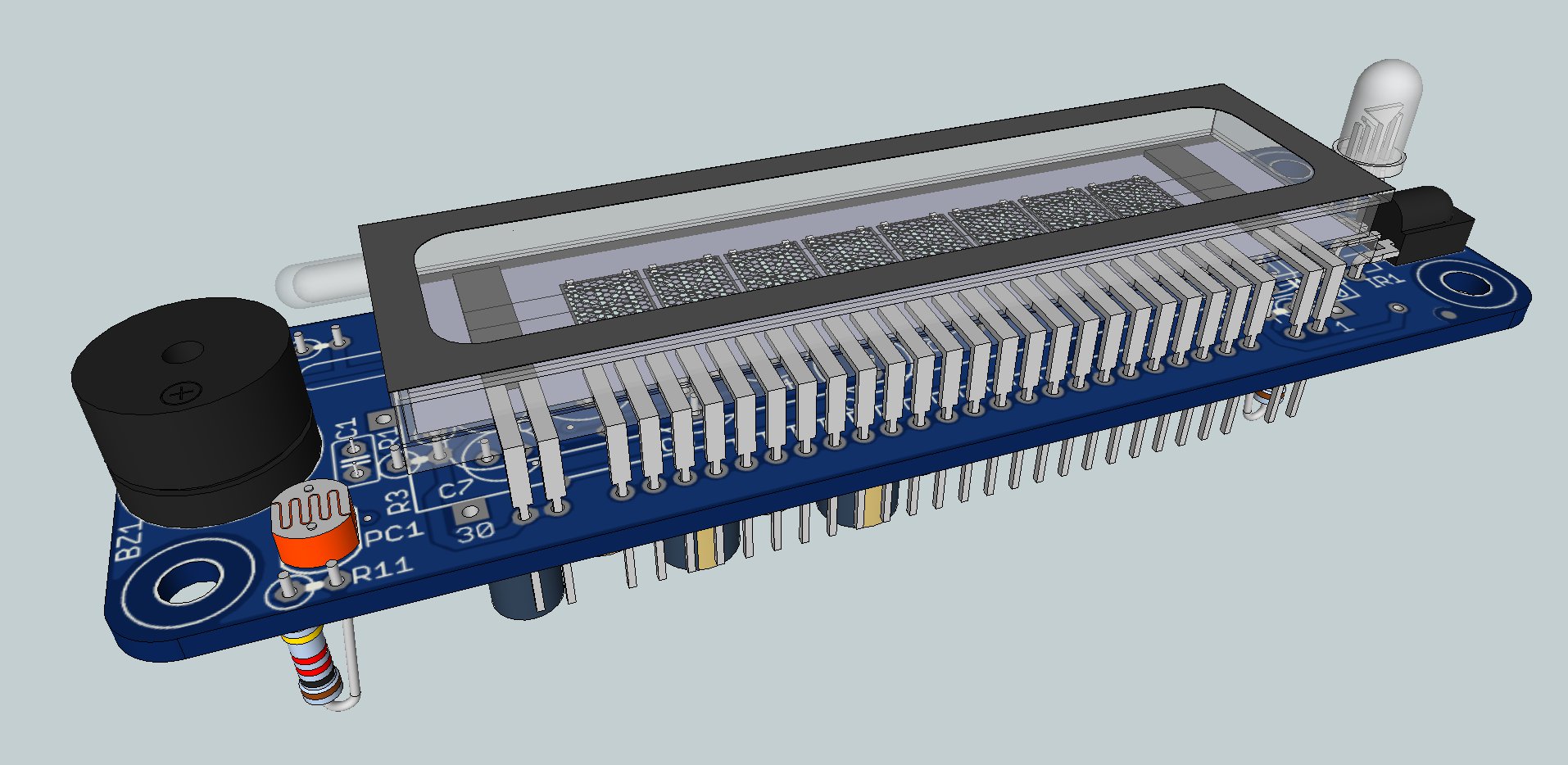
MVFDPanel 16S8D 3D Pic.#01
MVFDPanel 16S8D 3D Pic.#01
MVFDPanel 16S8D 3D Pic.#03
MVFDPanel 16S8D 3D Pic.#03

MVFDPanel 16S8D 3D Pic.#05
MVFDPanel 16S8D 3D Pic.#06

Leave a Reply
You must be logged in to post a comment.